01
Validation status and limitations
This English-only page is a calculated publication candidate, not a released schematic or qualified product. No Hengshun prototype, waveform, efficiency map, temperature map, EMI result, surge result or compliance report exists. Vendor EVM measurements are manufacturer context only and do not transfer to a Hengshun PCB.
Evidence boundary
- Bench validation: NOT EXECUTED
- Thermal characterization: NOT EXECUTED
- EMI and compliance testing: NOT EXECUTED
- Production and field qualification: NOT EXECUTED
- Full production BOM release readiness: NO
02
Design intent and end application
RD8 is a downstream, non-isolated point-of-load stage for industrial FPGA or ASIC compute. It converts an already regulated and protected intermediate bus into a sub-1 V core rail; it does not define the upstream supply, processor-specific sequencing, AVS behavior or board-level thermal solution.
- Application
- Industrial FPGA / ASIC compute
- Domain
- HIGH_CURRENT_POINT_OF_LOAD_FOR_INDUSTRIAL_FPGA_ASIC_COMPUTE
- Topology
- Two-phase interleaved synchronous buck module
- Design state
- CALCULATED_DESIGN
03
Protected intermediate-bus boundary
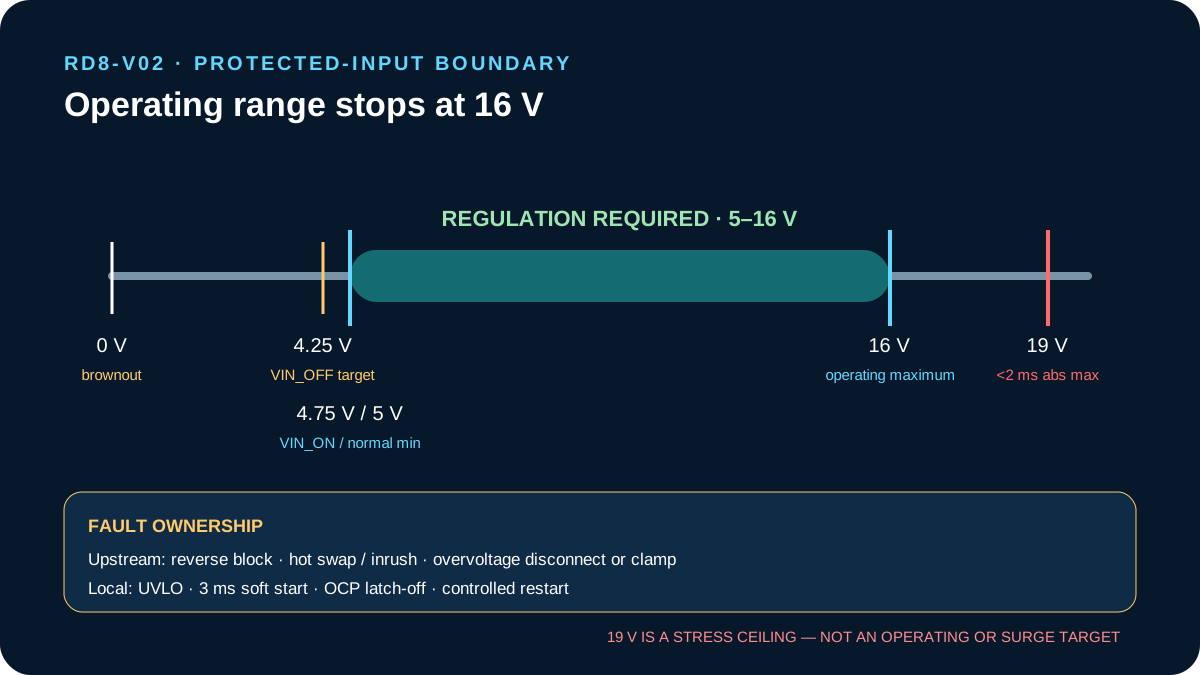
The locked operating node is 5–16 V, with 12 V nominal. A 0 V interruption is a brownout event that requires controlled shutdown and restart. The 19 V, less-than-2-ms absolute maximum is only a stress ceiling; operation above 16 V, surge survival and reverse-polarity tolerance are not claimed.
| Quantity | Locked value | Evidence class | Interpretation |
|---|---|---|---|
| Nominal input | 12 V | PROJECT_DESIGN_POINT | Protected intermediate bus |
| Normal input | 5–16 V | OFFICIAL_EXAMPLE / PROJECT_BOUNDARY | Regulation-required range |
| Brownout event | 0 V | PROJECT_DEFINED | Regulation not required; controlled restart |
| Absolute maximum | 19 V for <2 ms | OFFICIAL_DEVICE_FACT | Stress ceiling, not operating capability |
04
System power tree and sequencing ownership
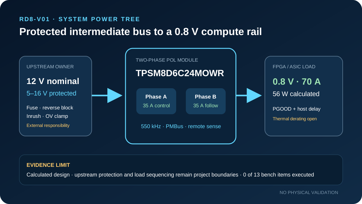
Protected 5–16 V intermediate bus → local PVIN bypass and bulk network → TPSM8D6C24 two-phase module → remote-sensed 0.8 V rail → FPGA or ASIC load. The upstream system owns reverse blocking, inrush and overvoltage containment; the load host owns reset, enable sequencing and application acceptance criteria.
05
TPSM8D6C24 selection and exact orderable identity
TPSM8D6C24 is an active dual-35 A PMBus buck power module that supports a stacked single 70 A output. The exact selected orderable is TPSM8D6C24MOWR in the 59-pin MOW package. Device production status does not make the complete RD8 implementation production ready.
06
Two-phase controller/follower architecture
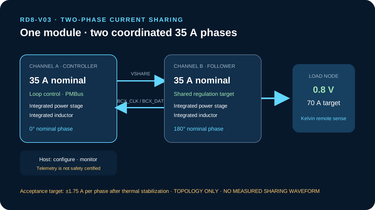
One module uses channel A as loop controller and channel B as follower. VSHARE carries the analog sharing signal while BCX_CLK and BCX_DAT coordinate phase operation; nominal interleaving is 180° at 550 kHz. Differential remote sense closes regulation at the load connection rather than at the module pads.
07
Duty-cycle and electrical margin calculations
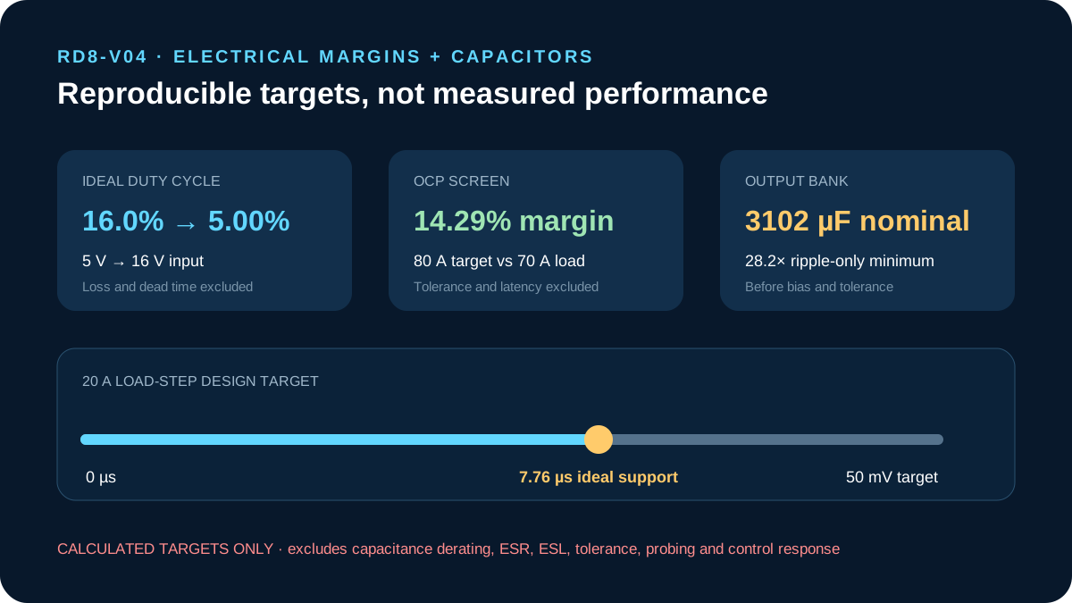
Ideal duty cycle is 16.0% at 5 V, 6.67% at 12 V and 5.00% at 16 V. The 80 A overcurrent target gives 14.29% nominal margin above the 70 A calculated load. These screens exclude loss, dead time, minimum-pulse behavior, command tolerance and transient response.
| Calculation | Inputs | Result | Limitation |
|---|---|---|---|
| Output power | 0.8 V × 70 A | 56 W | Excludes distribution loss |
| Per-phase current | 70 A / 2 | 35 A | Thermal derating may reduce release current |
| Ideal duty | 0.8 V / 5, 12, 16 V | 16.0%, 6.67%, 5.00% | Ideal approximation |
| OCP margin | (80 A − 70 A) / 70 A | 14.29% | Tolerance and delay excluded |
08
Current sharing, remote sense, and PMBus behavior
Each phase carries 35 A nominal at full load. The project acceptance target is no more than ±1.75 A mismatch per phase after thermal stabilization. PMBus may configure startup and faults and report voltage, current and die temperature, but its telemetry is not safety-certified and the final register image remains deferred.
09
Input and output capacitor strategy
The TI input method yields 31.8 µF minimum and 5.02 mΩ maximum ESR allocation without interleaving credit. The output starts at 3102 µF nominal; it is 28.2× the 110 µF ripple-only minimum because the 20 A load-step target dominates. Ideally, 3102 µF supports a 20 A step for 7.76 µs before 50 mV droop, excluding derating, ESR, ESL and control response.
10
Startup, brownout, overcurrent, and recovery policy
The target soft-start is 3 ms TON_RISE after configuration and enable conditions are valid. Project UVLO targets are 4.75 V on and 4.25 V off; brownout holds the load in reset. The intended 80 A fault response is immediate shutdown and latch-off, followed by a controlled host recovery after the cause is removed. All thresholds, timing and recovery behavior require EVM and hardware validation.
11
Loss, thermal, current-density, and layout screen
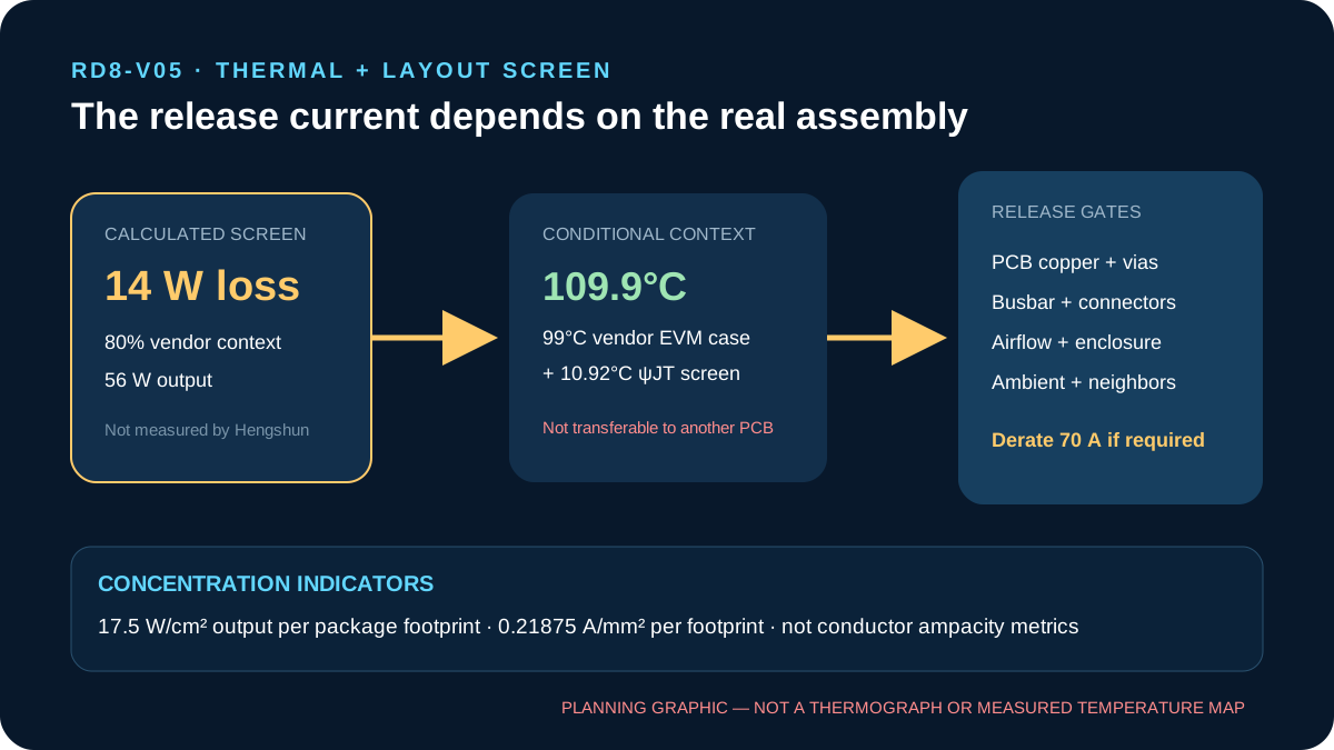
At the vendor example's 80% efficiency context, calculated input power is 70 W, input current is 5.83 A at 12 V and loss is 14 W. The 16 mm × 20 mm footprint corresponds to 17.5 W/cm² output-power density and 0.21875 A/mm² output current per package footprint. These are concentration indicators, not copper ampacity or measured thermal results.
Thermal release gate
- Vendor EVM case temperature and airflow are not transferable
- Copper stack-up, thermal vias, connector and busbar are deferred
- 70 A may require derating after board and enclosure validation
12
Critical BOM maturity
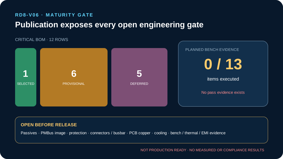
All twelve critical rows remain visible. Only TPSM8D6C24MOWR is selected; six electrical networks are provisional and five system or mechanical functions are deferred. Publication does not promote an unresolved row.
| ID | Function | Part or starting value | Status | Open evidence |
|---|---|---|---|---|
| B01 | Two-phase buck module | TPSM8D6C24MOWR | SELECTED | Target-PCB thermal derating |
| B02 | Per-phase ceramic input bypass | 8 × 22 µF / 25 V X7R | PROVISIONAL | Effective capacitance and ripple |
| B03 | Input bulk bank | 4 × 100 µF / 25 V low-ESR | PROVISIONAL | ESR, ripple, life and damping |
| B04 | High-frequency PVIN bypass | 6 × 6.8 nF / 25 V | PROVISIONAL | Package and placement parasitics |
| B05 | Output polymer bank | 4 × 470 µF | PROVISIONAL | Voltage, ESR, ripple and life |
| B06 | Output ceramic bank | 26 × 47 µF MLCC | PROVISIONAL | Bias, tolerance, ESR and ESL |
| B07 | PMBus / strap / sense passives | Network per reviewed register image | PROVISIONAL | Exact codes, values and alert policy |
| B08 | Upstream protection | TBD | DEFERRED | Source faults, inrush and overvoltage |
| B09 | Input power interconnect | TBD | DEFERRED | Temperature rise and fault rating |
| B10 | 0.8 V output interconnect / busbar | TBD | DEFERRED | 70 A drop and load distribution |
| B11 | PCB copper / via system | TBD | DEFERRED | Stack-up and electrothermal review |
| B12 | Cooling / airflow boundary | TBD | DEFERRED | Ambient, airflow and enclosure |
13
Planned bench validation
All thirteen items are plans only. Zero have been executed, and no item provides pass evidence.
- PLANNED_NOT_EXECUTED — BP01 current-limited 12 V bring-up, configuration, PGOOD and PMBus state
- PLANNED_NOT_EXECUTED — BP02 0.8 V static regulation at 5 V, 12 V and 16 V from 0 to 70 A
- PLANNED_NOT_EXECUTED — BP03 20 A load-step response against the 50 mV design target
- PLANNED_NOT_EXECUTED — BP04 80 A threshold, short-circuit shutdown, latch-off and recovery
- PLANNED_NOT_EXECUTED — BP05 3 ms startup, pre-bias, inrush and monotonicity
- PLANNED_NOT_EXECUTED — BP06 4.75 V on / 4.25 V off brownout targets and chatter-free restart
- PLANNED_NOT_EXECUTED — BP07 controlled protected-node events only within 0–16 V
- PLANNED_NOT_EXECUTED — BP08 upstream reverse-polarity block with module pins not reverse-biased
- PLANNED_NOT_EXECUTED — BP09 module, board, capacitor and interconnect thermal mapping
- PLANNED_NOT_EXECUTED — BP10 line/load efficiency and loss with declared uncertainty
- PLANNED_NOT_EXECUTED — BP11 ripple and noise at the load with bandwidth-limited probing
- PLANNED_NOT_EXECUTED — BP12 conducted and radiated EMI exploratory pre-scan
- PLANNED_NOT_EXECUTED — BP13 phase balance, telemetry, alerts, faults and recovery
14
Visual evidence boundary
Six local semantic diagrams explain architecture, ownership, calculations, thermal risk and maturity. They are code-native explanatory visuals, not PCB imagery, oscilloscope traces, thermographs, measured curves or compliance evidence.
| Visual ID | Purpose | Locked content | Limitation |
|---|---|---|---|
| RD8-V01 | System power tree | 5–16 V to 0.8 V / 70 A | Calculated architecture |
| RD8-V02 | Input boundary | 0 V, 5–16 V, 19 V <2 ms | Absolute maximum is not operation |
| RD8-V03 | Two-phase map | 2 × 35 A, 550 kHz, PMBus | No measured sharing waveform |
| RD8-V04 | Electrical margins | Duty, OCP, 3102 µF, 7.76 µs | Calculated targets only |
| RD8-V05 | Thermal screen | 14 W, conditional 109.9°C, 17.5 W/cm² | Vendor context not transferable |
| RD8-V06 | Maturity | 1 / 6 / 5 BOM and 0 of 13 tests | Not production-release evidence |
15
Official sources and related public engineering context
These Texas Instruments sources support device identity, operating limits, the two-phase example, capacitor method and EVM context. Related Hengshun pages provide upstream conversion and compute power-tree context only. No TPSM8D6C24 Component Guide or high-current POL Technical Guide is currently published.