01
Validation status and limitations
This record is a calculated engineering publication candidate. No released schematic, PCB, prototype, waveform, efficiency result, temperature result, surge result, reverse-polarity result, EMI result or compliance report has been produced for this design. Every physical result described below is planned rather than executed.
Evidence boundary before design claims
- Board validation: NOT EXECUTED
- Thermal and chamber validation: NOT EXECUTED
- Surge, reverse-polarity and protection validation: NOT EXECUTED
- EMI and compliance testing: NOT EXECUTED
02
Design scope and requirement boundary
The design converts a protected 24 V industrial distribution source to a 5 V / 3 A continuous rail. The selected values are a reproducible project design point informed by official sources; they are not universal industrial requirements and do not establish suitability for an installation without its wiring, fault-current and environmental requirements.
03
Input operating envelope
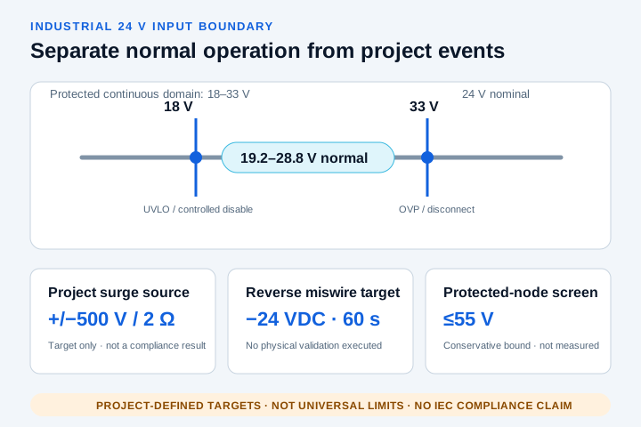
The nominal source is 24 VDC, the normal continuous range is 19.2–28.8 V, and the protected downstream operating boundary is 18–33 V. Sustained input above the 33 V OVP target is intended to be disconnected rather than presented to the buck as a normal operating condition.
- Nominal
- 24 VDC
- Normal continuous
- 19.2–28.8 V
- Protected continuous
- 18–33 V
- Conservative event bound
- ≤55 V · calculated screen
04
Brownout and recovery requirement
The project target is regulated 5 V / 3 A at or above the 18 V protected-input threshold, controlled disable below the threshold and automatic recovery when the source returns. Ride-through time, hysteresis, restart delay and output discharge behavior remain bench acceptance items rather than assumed performance.
05
Surge and reverse-polarity boundary
The source-side project events are +/−500 V with 2 Ω generator impedance and a −24 VDC steady reverse miswire for 60 s. The referenced TPS2663 example informs the architecture, but this publication candidate does not claim IEC 61000-4-5 compliance, dynamic survival, TVS energy closure or MOSFET safe-operating-area closure.
06
System power-tree architecture
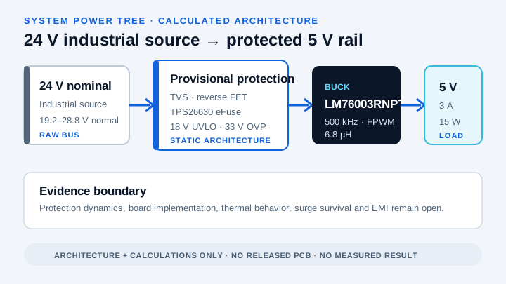
Raw 24 V bus → bidirectional TVS and reverse-blocking MOSFET → TPS26630 eFuse with 18 V UVLO, 33 V OVP and 2 A nominal limit → protected node → LM76003 synchronous buck → 5 V / 3 A load. The protected-node boundary prevents the raw surge source from being misrepresented as a regulator operating condition.
07
Protected-input front end
TPS26630RGER, CSD19537Q3, BSS138 and SMCJ36CA are provisional project parts derived from the official 24 V PLC protection example. Static identities and nominal thresholds are evidence-backed; dynamic overshoot, clamp tolerance, energy, SOA, trip behavior, thermal stress and restart behavior remain open.
- eFuse
- TPS26630RGER · provisional
- Reverse FET
- CSD19537Q3 · provisional
- TVS
- SMCJ36CA · provisional
- System fuse
- Deferred to installation coordination
08
Primary regulator selection
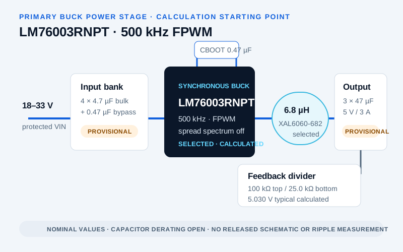
LM76003RNPT is selected for this calculated design because its 3.5–60 V operating range, 65 V absolute-maximum context, 3.5 A output capability and 4.35 A minimum high-side current limit cover the locked design point with positive calculated margin. The selection does not replace board-level qualification.
09
Operating mode and switching frequency
The locked stage operates at 500 kHz in fixed-frequency PWM with spread spectrum disabled. This operating point aligns with the official LM7600x evaluation-module BOM, while the thermal screen separately identifies that the nearby efficiency curve uses 400 kHz Auto mode and is not directly transferable.
10
Inductor and current-limit margin
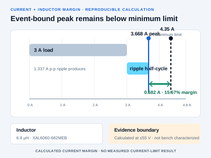
The selected XAL6060-682MEB value is 6.8 µH. At the conservative 55 V event-analysis bound, first-order ripple is 1.337 A p-p and peak current is 3.668 A, leaving 0.682 A or 15.67% to the 4.35 A guaranteed minimum current limit. These are reproducible calculations, not oscilloscope results.
11
Input capacitor strategy
Four 4.7 µF / 100 V C3225X7S2A475K200AB capacitors provide 18.8 µF nominal bulk capacitance and GRM31MR72A474KA35L provides 0.47 µF local high-frequency bypass. The bank remains provisional because exact effective capacitance at 33 V and temperature has not been established from vendor DC-bias evidence.
12
Output capacitor strategy
Three 47 µF / 10 V GRM32ER71A476KE15L capacitors provide 141 µF nominal capacitance against a ≥100 µF effective target. The bank remains provisional until voltage bias, temperature and ESR are confirmed; the 3.119–3.342 mV first-order capacitive ripple calculations exclude ESR, layout and control-loop effects.
13
Feedback and output-voltage tolerance
The nominal 100 kΩ / 25.0 kΩ divider produces 5.030 V at the 1.006 V typical feedback reference. Datasheet feedback limits alone give 4.935–5.085 V; a conservative independent 1% resistor stack expands the arithmetic screen to approximately 4.857–5.167 V before temperature coefficient and aging. This screen is not a measured regulation specification.
14
Bootstrap, compensation and startup
GRM188R61E474KA12D is the selected 0.47 µF / 25 V bootstrap capacitor, compensation is internal and the regulator's 6.3 ms internal soft-start is the starting point. Startup monotonicity, eFuse power-good handoff, inrush and load-specific startup must be verified on hardware.
15
Efficiency evidence boundary
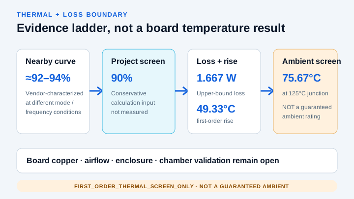
The official nearby 24 V / 5 V / 3 A curve is visually approximated at about 92–94%, but it is shown at 400 kHz Auto mode. The 500 kHz FPWM project uses 90% only as a deliberately conservative calculation screen; neither number is a measured efficiency result for this design.
16
First-order thermal screen
At 15 W output and the 90% efficiency screen, total converter loss is 1.667 W. Assigning all of that loss to the IC and multiplying by the datasheet 29.6°C/W metric gives a 49.33°C rise and a 75.67°C ambient screen for a 125°C junction. Actual PCB copper, airflow, enclosure and loss split must be measured.
FIRST_ORDER_THERMAL_SCREEN_ONLY
- 75.67°C is not a guaranteed maximum ambient.
- Board thermal mapping and chamber validation are required.
- Inductor, capacitors, eFuse, reverse FET and TVS also require temperature observation.
17
Critical BOM
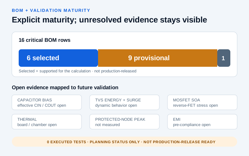
The publication-candidate BOM contains exactly sixteen critical rows. Six are selected for the calculated design, nine remain provisional and the upstream branch fuse or breaker remains deferred. Maturity is explicit so that a candidate part number is not mistaken for production release.
| ID | Function | Manufacturer part | Maturity |
|---|---|---|---|
| BOM-001 | Primary synchronous buck | LM76003RNPT | SELECTED_CALCULATED |
| BOM-002 | Power inductor | XAL6060-682MEB | SELECTED_EVIDENCE_BACKED |
| BOM-003 | Input bulk bank · 4 pieces | C3225X7S2A475K200AB | PROVISIONAL |
| BOM-004 | High-frequency input bypass | GRM31MR72A474KA35L | SELECTED_EVIDENCE_BACKED |
| BOM-005 | Output bank · 3 pieces | GRM32ER71A476KE15L | PROVISIONAL |
| BOM-006 | Feedback top · 100 kΩ | CRCW0603100KFKEA | SELECTED_CALCULATED |
| BOM-007 | Feedback bottom · 25.0 kΩ | PROVISIONAL_25K0_1PCT_0603 | SELECTED_CALCULATED |
| BOM-008 | Bootstrap capacitor | GRM188R61E474KA12D | SELECTED_EVIDENCE_BACKED |
| BOM-009 | Front-end eFuse | TPS26630RGER | PROVISIONAL |
| BOM-010 | Reverse-polarity MOSFET | CSD19537Q3 | PROVISIONAL |
| BOM-011 | Gate pull-down MOSFET | BSS138 · exact vendor TBD | PROVISIONAL |
| BOM-012 | Bidirectional surge TVS | SMCJ36CA · exact vendor TBD | PROVISIONAL |
| BOM-013 | eFuse current-limit resistor | 9.09 kΩ / 1% · exact MPN TBD | PROVISIONAL |
| BOM-014 | eFuse UV/OV divider | 887 kΩ / 29.4 kΩ / 34 kΩ · exact MPNs TBD | PROVISIONAL |
| BOM-015 | eFuse dV/dt capacitor | 100 nF · exact MPN TBD | PROVISIONAL |
| BOM-016 | Upstream branch fuse or breaker | SYSTEM_LEVEL_TBD | DEFERRED |
18
BOM convergence result
All ten non-final HGS37 rows were reviewed once. CIN and COUT remain provisional because exact effective-capacitance evidence is unresolved; protection rows remain provisional because dynamic coordination and exact supporting MPNs are open; the branch fuse remains deferred because installation wiring and available fault current are system inputs.
- CIN DC-bias status
- PROVISIONAL · exact 33 V effective value open
- COUT DC-bias status
- PROVISIONAL · exact 5 V effective value open
- Inductor margin status
- PASS calculated · thermal curves open
- Front-end coordination
- PROVISIONAL · dynamic stress validation open
19
Layout and grounding priorities
Place the TVS and surge-current return at the connector boundary, keep the eFuse and reverse-FET current path short, and isolate that stress loop from signal ground. At the buck, place the 0.47 µF input bypass and bootstrap loop tightly, minimize switch-node area and use quiet Kelvin-style feedback routing.
20
EMI planning boundary
The publication candidate identifies high-di/dt loops and reserves space for damping or filtering, but it does not select a final input filter without a source-impedance model. Conducted emissions, radiated emissions, immunity and filter stability require defined limits and physical pre-compliance work.
21
Planned bench validation
The validation plan is intentionally unexecuted. It covers pre-power inspection; line/load regulation; startup and shutdown; brownout and recovery; load steps; ripple; efficiency; current limit; short circuit; thermal mapping; reverse polarity; approved surge testing; protected-node overshoot; TVS energy; MOSFET SOA; and later EMI pre-compliance.
- PLANNED / NOT EXECUTED — steady-state 18, 19.2, 24, 28.8 and 33 V line/load matrix
- PLANNED / NOT EXECUTED — startup, shutdown, inrush, UVLO, OVP and recovery
- PLANNED / NOT EXECUTED — ripple, efficiency, load transient and current-limit characterization
- PLANNED / NOT EXECUTED — thermal mapping and chamber evaluation
- PLANNED / NOT EXECUTED — reverse polarity, surge, TVS energy and MOSFET SOA
- PLANNED / NOT EXECUTED — conducted-noise observation and EMI pre-compliance
22
Visual evidence boundary
Six source-backed engineering visuals summarize locked requirements, official-source identities and reproducible calculations. They are publication-candidate diagrams only; none represents a measured result, certified compliance, released PCB or completed physical test.
| Visual ID | Purpose | Permitted content | Boundary |
|---|---|---|---|
| VIS-001 | System power tree | 24 V bus → protection → LM76003 → 5 V / 3 A | AVAILABLE_CALCULATED_ONLY |
| VIS-002 | Input boundary | 19.2–28.8 V; 18 V UVLO; 33 V OVP; project surge | AVAILABLE_CALCULATED_ONLY |
| VIS-003 | Buck power stage | LM76003RNPT; 6.8 µH; capacitor banks; divider | AVAILABLE_CALCULATED_ONLY |
| VIS-004 | Current margin | 1.337 A p-p; 3.668 A; 4.35 A; 0.682 A / 15.67% | AVAILABLE_CALCULATED_ONLY |
| VIS-005 | Thermal boundary | 90% screen; 1.667 W; 49.33°C; 75.67°C | AVAILABLE_CALCULATED_ONLY |
| VIS-006 | BOM and validation maturity | 6 selected; 9 provisional; 1 deferred; open tests | AVAILABLE_CALCULATED_ONLY |
23
Official evidence and related engineering context
The official sources below support the regulator, evaluation-module values and protection architecture. The related LM5161-Q1, LMR38020-Q1 and LM5012-Q1 public guides are voltage-domain and topology context only; they are not LM76003 device guides and no internal LM76003 component route is asserted.