01
Validation status and limitations
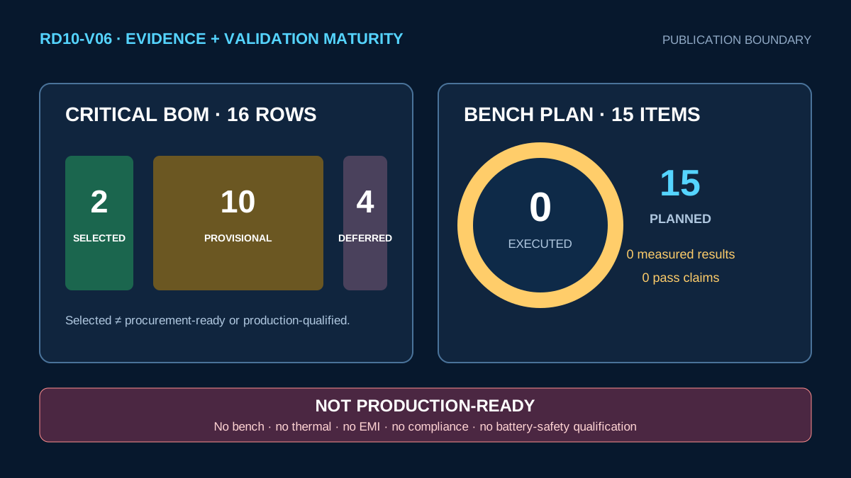
This English-only page is a calculated publication candidate, not a released schematic, validated charger or qualified product. No Hengshun hardware, waveform, efficiency map, thermal map, EMI result, battery-safety result or compliance report exists. TI EVM evidence is vendor context and is not transferable to a future Hengshun board.
Evidence boundary
- Board and bench validation: NOT EXECUTED
- Thermal characterization: NOT EXECUTED
- EMI and compliance testing: NOT EXECUTED
- Measured efficiency and transient response: NOT COLLECTED
- Battery pack safety qualification: OUTSIDE THIS DESIGN
- Production readiness: NO
02
Design intent and system boundary
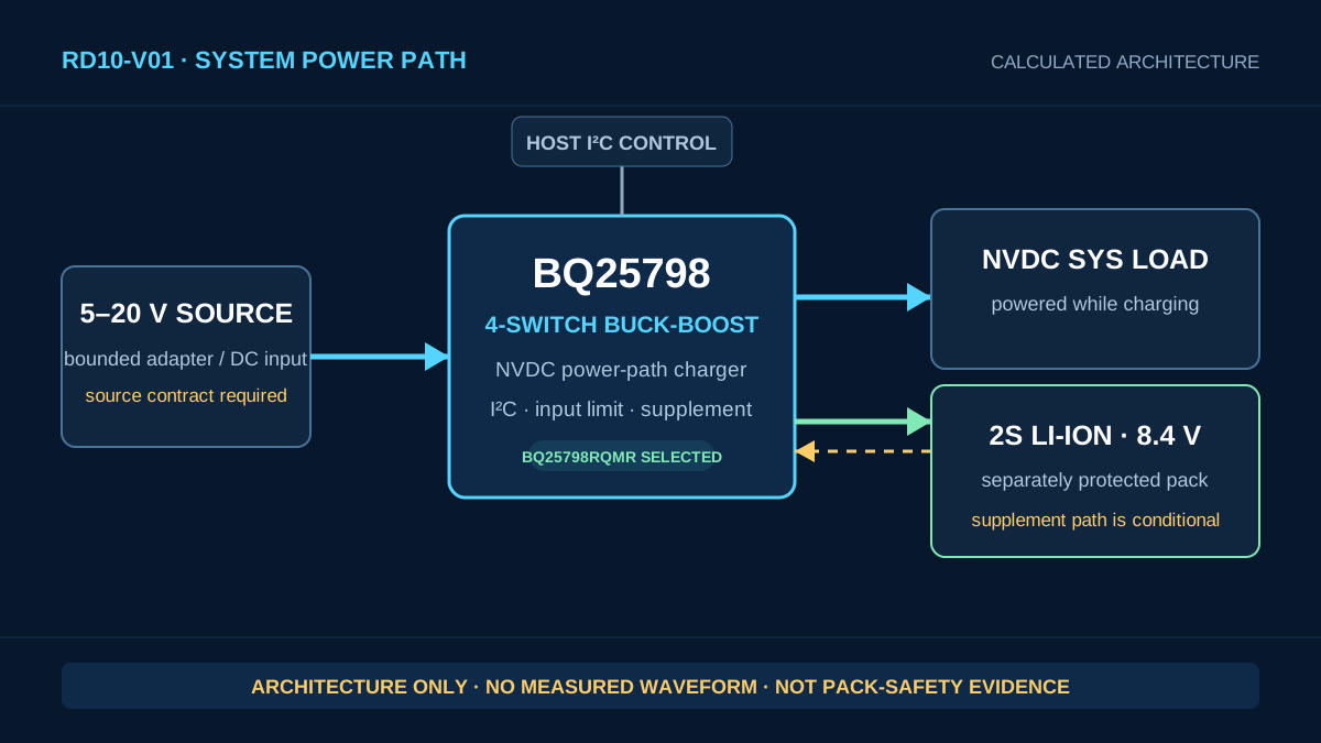
RD10 defines a BQ25798 charging and power-path starting point for portable or industrial battery-powered equipment. A bounded source feeds the charger, the NVDC SYS rail powers the system load, and a separately protected 2S pack charges or supplements the system. Source negotiation, cell protection, fuel gauging and end-product safety are outside this stage.
- Domain
- Portable and industrial battery-powered equipment
- Application
- 2S charging and NVDC system power
- Design state
- CALCULATED_DESIGN
- Isolation
- None · non-isolated
03
Official vendor context and device identity
Texas Instruments identifies BQ25798 as an I2C-controlled buck-boost charger with an NVDC power path for one-to-four-cell batteries. The selected orderable is BQ25798RQMR. The 1.5 MHz switching context, EVM application networks and SPM6530T-1R0M120 inductor originate in official TI materials; none is a Hengshun measurement.
04
NVDC power-path behavior
The adapter path feeds PMID and the four-switch converter, which regulates the SYS rail relative to the battery. The system can operate while the pack charges, charge current can reduce when source power is limited, and the battery can supplement the system when demand exceeds the allowed input. Exact priorities, thresholds and transitions remain configuration and bench work.
05
Four-switch buck-boost stage
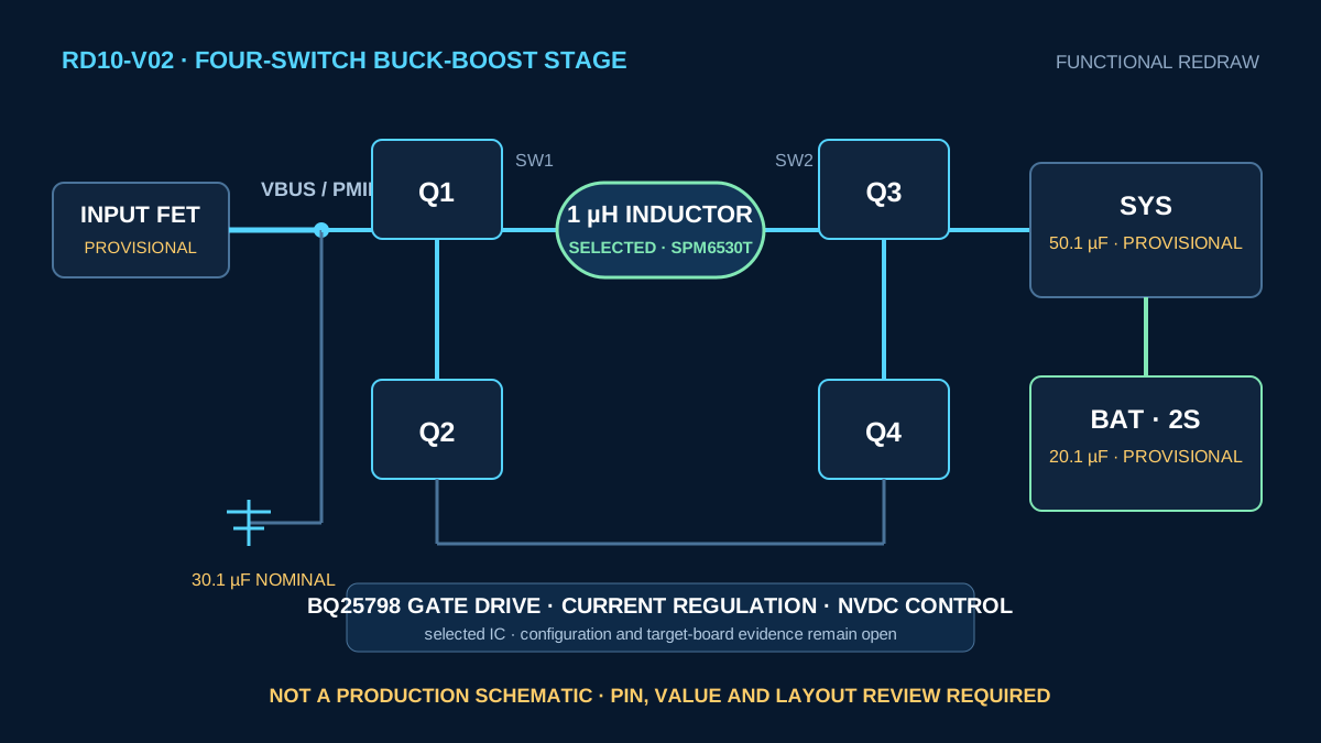
Two switching half-bridges surround the selected 1 µH inductor so the converter can boost below the battery/system region, transition near it and buck above it. PMID, SYS and BAT capacitor banks are provisional. The visual is a functional redraw, not a pin-complete or construction-ready schematic.
06
Fourteen reproducible calculation screens
Every result below is Hengshun calculated design guidance. The equations are first-pass analytical screens, not simulated or measured performance, and the declared assumptions and exclusions remain binding.
| ID | Inputs / equation | Result | Status and limitation |
|---|---|---|---|
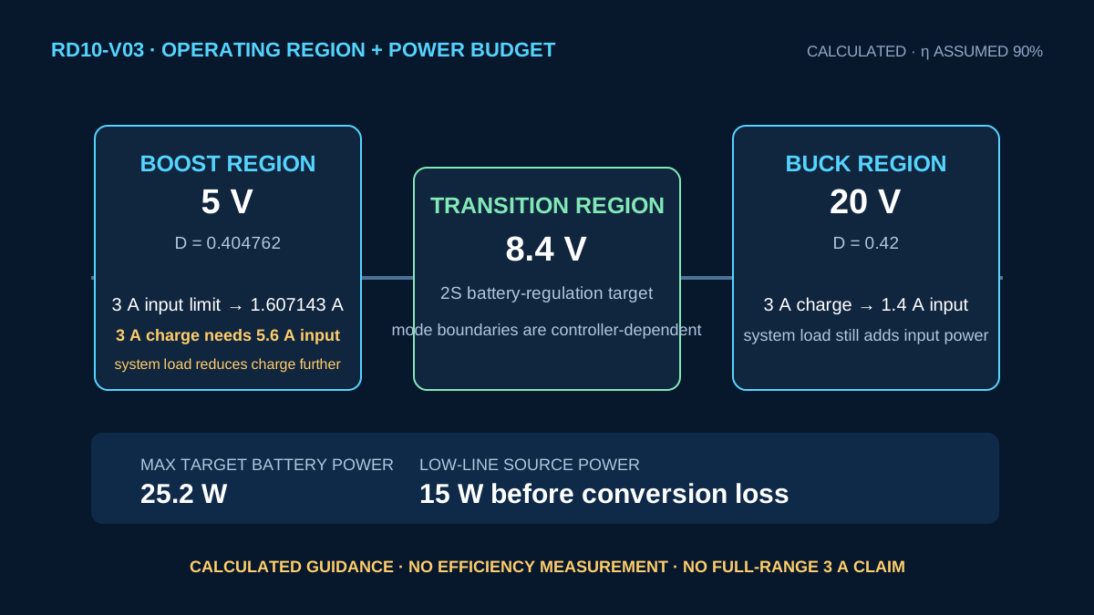
| C01 | 8.4 V × 3 A | 25.2 W | Calculated battery charge power; system load and loss excluded |
| C02 | 8.4 V / 20 V | 0.42 ratio | Ideal high-line buck duty |
| C03 | 1 − 5 V / 8.4 V | 0.404762 ratio | Ideal low-line boost duty |
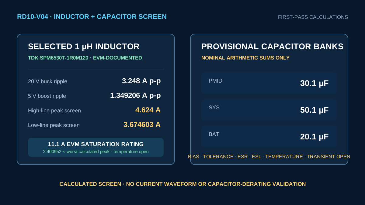
| C04 | 8.4 V × (1−0.42) / (1 µH × 1.5 MHz) | 3.248 A p-p | Ideal high-line ripple screen |
| C05 | 5 V × 0.404762 / (1 µH × 1.5 MHz) | 1.349206 A p-p | Ideal low-line ripple screen |
| C06 | 5 V × 3 A × 0.90 / 8.4 V | 1.607143 A | Low-line source-limited charge; zero system load assumed |
| C07 | 8.4 V × 3 A / (5 V × 0.90) | 5.6 A | Input required for 3 A charge at 5 V; exceeds 3 A source |
| C08 | 8.4 V × 3 A / (20 V × 0.90) | 1.4 A | Input required for 3 A charge at 20 V |
| C09 | 3 A + 1.349206 A / 2 | 3.674603 A | Ideal low-line peak screen |
| C10 | 3 A + 3.248 A / 2 | 4.624 A | Ideal high-line peak screen |
| C11 | 11.1 A / 4.624 A | 2.400952 ratio | EVM inductor rating ratio; temperature and tolerance open |
| C12 | 0.1 µF + 3 × 10 µF | 30.1 µF nominal | PMID arithmetic sum; derating excluded |
| C13 | 0.1 µF + 5 × 10 µF | 50.1 µF nominal | SYS arithmetic sum; transient adequacy open |
| C14 | 0.1 µF + 2 × 10 µF | 20.1 µF nominal | BAT arithmetic sum; pack impedance open |
07
Low-line source-limited behavior
At 5 V and a 3 A source limit, an explicit 90% planning assumption gives approximately 1.607143 A battery current before system load. Reaching 3 A battery charge at the same input would require about 5.6 A. Firmware and hardware limits must therefore prioritize source safety and system load instead of promising 3 A charge across the full range.
08
Magnetics, capacitors and unresolved margins
The selected EVM-documented 1 µH inductor provides a reproducible starting point, while current ripple, peak current and the 11.1 A rating ratio remain calculation screens. All three capacitor banks require effective-capacitance, ESR, ESL, bias, temperature, ripple and transient review on the target layout.
09
Critical BOM maturity
The Stage A split is preserved exactly: two selected rows, ten provisional rows and four deferred rows. A selected row supports this calculation starting point; it does not make the assembly procurement-ready or production-ready.
| ID | Function | Part or starting value | Status | Open evidence |
|---|---|---|---|---|
| B01 | Buck-boost charger and NVDC path | BQ25798RQMR | SELECTED | Target-board thermal and functional validation |
| B02 | Power inductor | TDK SPM6530T-1R0M120 · 1 µH · 11.1 A EVM rating | SELECTED | Tolerance, temperature, saturation and layout |
| B03 | PMID capacitor network | 0.1 µF + 3 × 10 µF | PROVISIONAL | Dielectric, bias, ripple and placement |
| B04 | SYS capacitor network | 0.1 µF + 5 × 10 µF | PROVISIONAL | Effective capacitance and transient response |
| B05 | BAT capacitor network | 0.1 µF + 2 × 10 µF | PROVISIONAL | Pack lead and hot-plug behavior |
| B06 | REGN decoupling | 4.7 µF starting value | PROVISIONAL | Rating, package and placement |
| B07 | Bootstrap capacitors | 47 nF × 2 | PROVISIONAL | Rating, dielectric and layout |
| B08 | ILIM_HIZ hardware limit | Network value TBD | PROVISIONAL | Equation and tolerance stack |
| B09 | Battery temperature sensing | Pack-qualified NTC network | PROVISIONAL | NTC curve, JEITA profile and thresholds |
| B10 | I2C / interrupt interface | Host-compatible pull-up network | PROVISIONAL | Host rail, capacitance and fault policy |
| B11 | Hot-plug damping / protection | Optional snubber or TVS | PROVISIONAL | Source impedance, surge target and energy |
| B12 | Input adapter FET | Single-source adapter-path implementation | PROVISIONAL | SOA, RDS(on), reverse behavior and thermal rise |
| B13 | 2S pack protection and fuse | Pack-qualified system | DEFERRED | Cell limits, safety and fuse coordination |
| B14 | Input connector and cable | Rated source interconnect | DEFERRED | Heating, cycles and source contract |
| B15 | Ship / system-load disconnect | Optional external switch | DEFERRED | State machine, leakage and safety |
| B16 | PCB thermal path and enclosure | Stack-up, copper, vias and airflow TBD | DEFERRED | Thermal model and enclosure testing |
10
Planned bench validation
The evidence plan contains fifteen future items and zero executed items. The list records what must be measured later and does not contain a pass result.
- PLANNED_NOT_EXECUTED — BP-01 Pre-power inspection of the as-built schematic, BOM, polarity, resistance and continuity before energization.
- PLANNED_NOT_EXECUTED — BP-02 Current-limited bring-up at 5 V, 9 V, 12 V, 15 V and 20 V with a battery simulator and conservative source limits.
- PLANNED_NOT_EXECUTED — BP-03 Input and charge-current sweep with the programmed input limit up to 3 A and the charge command bounded by available power.
- PLANNED_NOT_EXECUTED — BP-04 CC/CV charge profile across representative 2S pack states below, near and at the 8.4 V target.
- PLANNED_NOT_EXECUTED — BP-05 NVDC system-load sweep with and without simultaneous battery charging.
- PLANNED_NOT_EXECUTED — BP-06 Battery supplement-mode exercise when system demand exceeds the allowed input power.
- PLANNED_NOT_EXECUTED — BP-07 Controlled adapter insertion and removal with VBUS, PMID, VSYS and VBAT waveform capture.
- PLANNED_NOT_EXECUTED — BP-08 Low-line power-limit behavior at 5 V and a 3 A input-current limit without assuming 3 A battery charge.
- PLANNED_NOT_EXECUTED — BP-09 Inductor-current and switch-node observation in boost, transition and buck operating regions.
- PLANNED_NOT_EXECUTED — BP-10 Ripple and noise measurement with declared bandwidth and low-inductance probing.
- PLANNED_NOT_EXECUTED — BP-11 Thermal characterization at selected worst-case source, charge and system-load points.
- PLANNED_NOT_EXECUTED — BP-12 Fault and recovery checks for bounded input, battery, load, NTC and short-circuit conditions.
- PLANNED_NOT_EXECUTED — BP-13 I2C, interrupt and watchdog behavior with a reproducible register image and safe-state review.
- PLANNED_NOT_EXECUTED — BP-14 Efficiency and loss mapping across the approved 5/9/12/15/20 V matrix with measurement uncertainty.
- PLANNED_NOT_EXECUTED — BP-15 Exploratory conducted and radiated EMI pre-scan with no compliance claim.
11
Visual evidence boundary
Six original code-native SVGs explain architecture, the four-switch stage, calculated operating regions, component screens, placement priorities and evidence maturity. They contain no stock imagery, fabricated waveforms, thermographs, measured curves or compliance evidence.
- RD10-V01 — System power path · architecture only; no measured waveform
- RD10-V02 — Four-switch charging stage · not a production schematic
- RD10-V03 — Operating regions and power budget · calculated guidance
- RD10-V04 — Inductor and capacitor screens · derating remains open
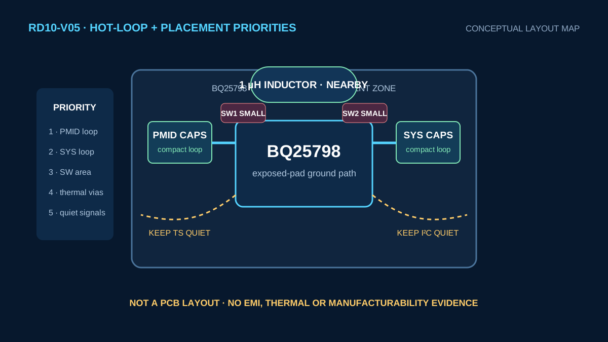
- RD10-V05 — Hot-loop placement priorities · not a PCB or EMI result
- RD10-V06 — BOM and validation maturity · not production readiness
12
Relationship implementation plan
Five reviewed conversion or navigation paths are available. Two missing content types remain explicit non-links, two future topics remain discovery-only, and localized editions remain deferred.
| ID | Target | Public action | Status |
|---|---|---|---|
| R01 | Battery Charging & Power Path | Primary solution relationship | RESOLVED_LINK |
| R02 | DC-DC Power Conversion | Secondary solution relationship | RESOLVED_LINK |
| R03 | BMS Power | Application relationship | RESOLVED_LINK |
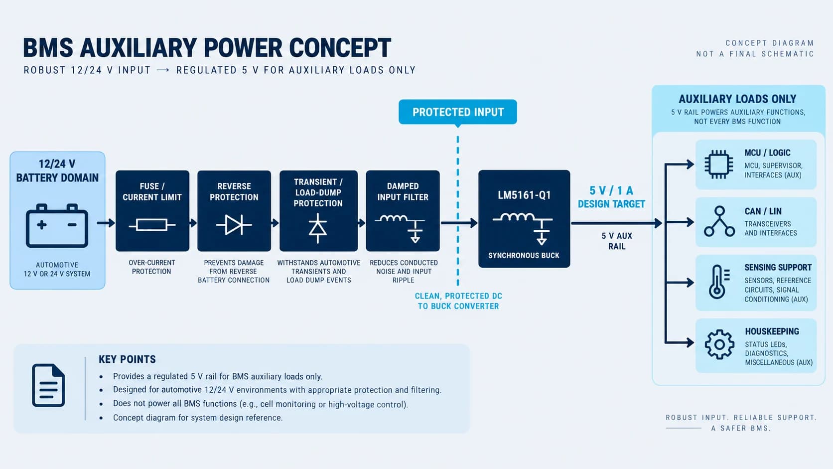
| R04 | BMS Auxiliary Power Reference Design | Related design card | RESOLVED_LINK |
| R05 | Request a Design | Existing engineering CTA | RESOLVED_LINK |
| R06 | BQ25798 Component Guide | Plain text only; page does not exist | EXPLICIT_NO_LINK |
| R07 | Battery charger selection guide | No card until separately published | EXPLICIT_NO_LINK |
| R08 | USB Type-C / USB-PD source integration | Editorial discovery only | DISCOVERY_ONLY |
| R09 | 2S protector, gauge and monitor | Future subsystem discovery only | DISCOVERY_ONLY |
| R10 | Localized RD10 editions | No placeholder translations | DEFERRED |
13
Official sources
First-party Texas Instruments sources support device identity, application behavior, orderable identity, EVM networks and vendor reference context. The TIDA source provides adjacent reference context only. Vendor material does not establish Hengshun board performance.
14
Related public engineering context
The reviewed links connect RD10 to Battery Charging & Power Path, DC-DC Power Conversion, BMS Power and the BMS auxiliary supply design. Project-specific pack, source and system-load requirements can proceed through Request a Design. Missing component-guide and technical-guide pages are intentionally not fabricated.