01
At a glance
02
What this design is
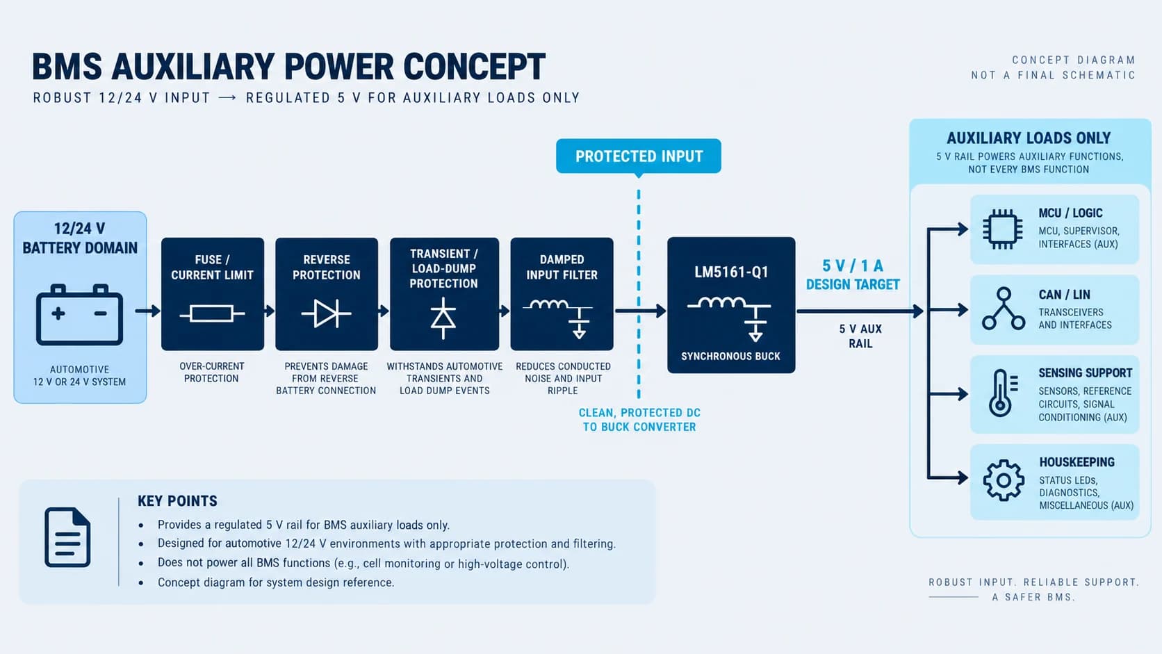
This record turns a defined BMS auxiliary-power question into a concrete calculation package: a protected 12/24 V battery-domain source is stepped down to a 5 V / 1 A rail for monitoring, communications, control and housekeeping loads. The page exposes assumptions, selected parts, calculated margins and open evidence gates so an engineer can review the reasoning rather than infer completeness from a schematic.
03
What this design is not
Publication does not make the circuit production ready
- No simulation result is claimed.
- No prototype, efficiency, ripple, thermal or EMI measurement exists.
- No automotive, ISO, CISPR or other compliance result is claimed.
- The upstream vehicle fuse, reverse-polarity stage, clamp/disconnect and filter remain system dependent.
04
Input-domain boundaries
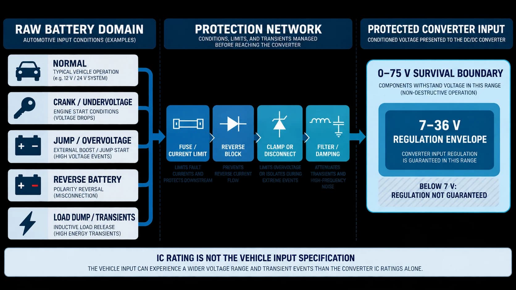
Raw battery voltage is not protected VIN. Vehicle events must first pass through a project-specific protection system. This converter is designed to regulate from 7 V through 36 V at the protected node. From above 36 V through 75 V, the requirement is survival only: continued 5 V regulation is not promised. Below 7 V the output may droop until nominal 6.582 V falling UVLO creates a controlled shutdown.
05
Power architecture
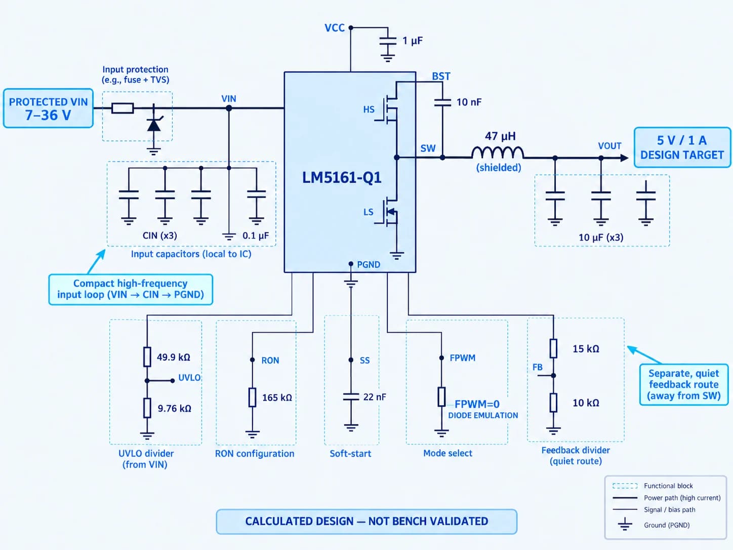
The selected Option A boundary keeps the raw vehicle-energy problem upstream and treats the LM5161-Q1 stage as a protected-input converter. Local high-frequency input capacitance, the integrated synchronous switches, 47 µH inductor, output bank, feedback, UVLO, RON and soft-start networks form the reviewable converter stage.
06
Why LM5161-Q1
The device provides the 100 V class, integrated synchronous switches, 1 A output capability and constant-on-time architecture needed for the protected-input envelope. It is selected for this calculation, not declared universally suitable. LM5012-Q1 is alternate-only and would require its own calculation, magnetics, BOM and validation package.
QuestionWhich regulator anchors this design?
SelectedLM5161-Q1.
WhyIt covers the protected VIN boundary and the 5 V / 1 A target with integrated synchronous switching.
EvidenceTI LM5161-Q1 data sheet E1; timing and current-margin calculations below.
07
Electrical design decisions
QuestionHow is switching frequency set?
Selected165 kΩ RON, 300.625301 kHz nominal.
WhyThis stays close to the 300 kHz starting point while retaining timing margin at both VIN limits.
EvidenceCalculated 950.4 ns off-time at 7 V and 462 ns on-time at 36 V.
QuestionWhich light-load mode is used?
SelectedDiode-emulation, FPWM pin low.
WhyIt avoids forced-CCM light-load loss for BMS housekeeping loads.
EvidenceManufacturer mode guidance E1; light-load frequency behavior remains an EMI test item.
QuestionHow is startup controlled?
Selected22 nF soft-start capacitor, about 4.4 ms.
WhyIt creates a deliberate starting ramp without claiming measured inrush.
EvidenceLM5161-Q1 equation and KEMET capacitor evidence E11.
QuestionWhere does the converter switch off?
Selected7.579754 V rising and 6.581754 V falling nominal UVLO.
WhyThe threshold distinguishes regulation from degraded operation and controlled reset.
Evidence49.9 kΩ / 9.76 kΩ network calculated from E1 and evidenced by E10.
08
Magnetics and current margin
| Protected VIN | Ripple current | Peak current |
|---|---|---|
| 7 V | 0.101106 A | 1.050553 A |
| 12 V | 0.206426 A | 1.103213 A |
| 24 V | 0.280149 A | 1.140074 A |
| 36 V | 0.304723 A | 1.152362 A |
At low inductance and low switching-frequency tolerance, the worst calculated peak is 1.192357 A. That is 0.107643 A, or 8.28%, below the device’s 1.3 A minimum current limit. The inductor’s 2.5 A saturation rating remains 0.600 A, or 31.58%, above the device’s 1.9 A maximum current limit.
09
Capacitor strategy
The local input network uses one 0.1 µF / 100 V X7R high-frequency bypass plus three 2.2 µF / 100 V X7R capacitors. Its 3.696 µF effective design floor is 2.22× the 1.663 µF calculated minimum. The output uses three 10 µF / 25 V X7R capacitors; the 20.25 µF effective floor gives an approximately 9.3 mV analytical ripple estimate before parasitic and measurement effects.
10
Selected BOM
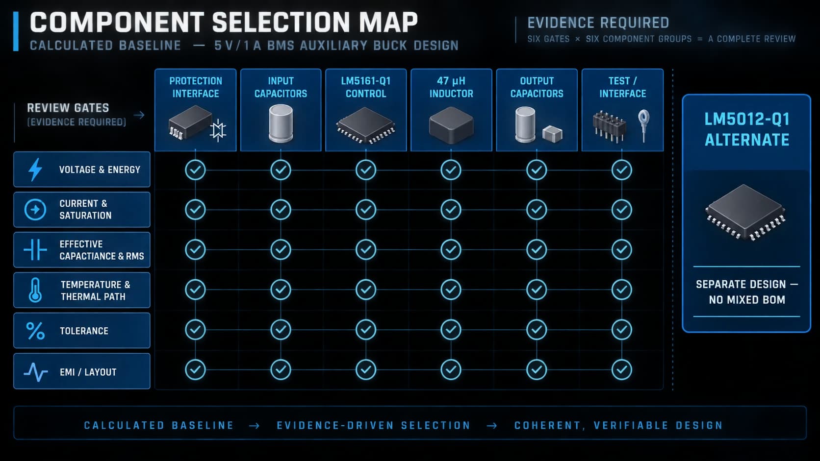
Thirteen rows have a concrete manufacturer part and primary-source evidence. Two system-interface rows remain deliberately provisional because their values depend on the vehicle event, source impedance and EMI requirements.
| Ref. | Manufacturer part | Selected value / role | Status |
|---|---|---|---|
| U1 | LM5161QPWPRQ1 | 100 V / 1 A synchronous buck | Selected |
| L1 | XGL6060-473MEC | 47 µH | Selected |
| C1 | C0603C104K1RACAUTO | 0.1 µF / 100 V X7R | Selected |
| C2–C4 | C1210X225M1RACAUTO | 3 × 2.2 µF / 100 V X7R | Selected |
| C5–C7 | C1206C106K3RACAUTO | 3 × 10 µF / 25 V X7R | Selected |
| R1 | CRCW060315K0FKEA | 15.0 kΩ / 1% | Selected |
| R2 | CRCW060310K0FKEA | 10.0 kΩ / 1% | Selected |
| R3 | CRCW0603165KFKEA | 165 kΩ / 1% | Selected |
| R4 | CRCW060349K9FKEA | 49.9 kΩ / 1% | Selected |
| R5 | CRCW06039K76FKEA | 9.76 kΩ / 1% | Selected |
| C8 | C0603C223K5RACAUTO | 22 nF / 50 V X7R | Selected |
| C9 | C0603C105K4RACAUTO | 1 µF / 16 V X7R | Selected |
| C10 | C0603C103K5RACAUTO | 10 nF / 50 V X7R | Selected |
| FL1 | System dependent | Optional damped input EMI filter | Provisional |
| J1 | System dependent | Protected-input interface | Provisional |
11
Layout and EMI priorities
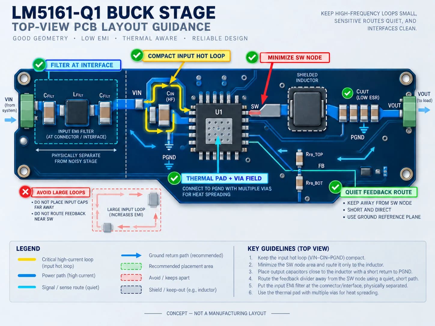
Place the 0.1 µF bypass and local input bank directly across VIN and PGND, minimize the hot-loop area and switch-node copper, keep the inductor and output return compact, and route feedback away from switching fields. Join signal and power grounds deliberately. Keep the connector-side filter physically outside the local converter loop, then select and damp it only after the source impedance and conducted-noise target are known.
12
Thermal and efficiency status
The partial analytical loss subtotal is 0.489 W at 12 V, 0.418 W at 24 V and 0.394 W at 36 V for high-side conduction, low-side conduction and inductor DCR only. It excludes switching loss, gate drive, quiescent current, temperature-dependent resistance, core loss and the PCB-to-ambient path. No efficiency curve or junction-temperature claim is made.
13
Validation plan
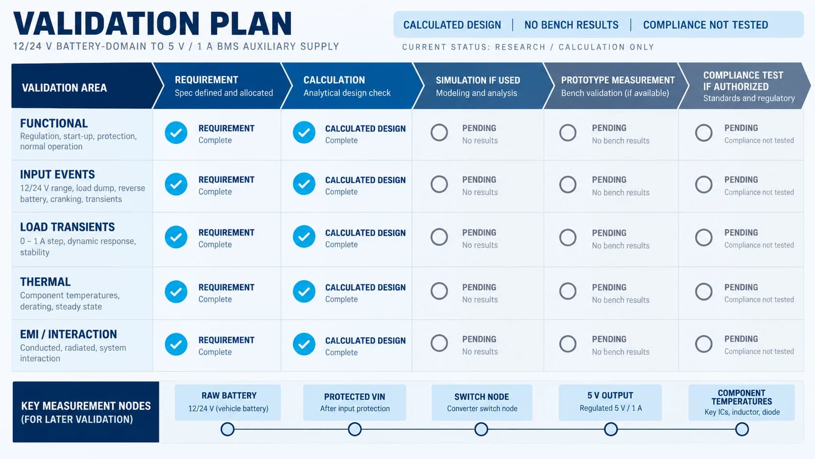
Next evidence should verify regulation and ripple across line and load, startup and shutdown, source dips and residual high-voltage events, load steps, current limit and short-circuit recovery, component and PCB temperature, conducted and radiated interaction, and noise coupling into BMS measurement and communications. Conditions, probes and acceptance limits must be recorded with every result.
- Simulation: control, startup, load-step and tolerance behavior where a validated model is available.
- Prototype measurement: electrical performance, fault recovery and component stress on the intended PCB.
- Thermal review: production stackup, enclosure, ambient and neighboring heat sources.
- Compliance: only under separately authorized system-level requirements and test plans.
14
Official-source references
- E1: Texas Instruments — LM5161-Q1 data sheet ↗
- E2: TI TIDA-01167 reverse-polarity and load-dump protection reference design ↗
- E3: TI automotive 24 V battery input protection and power architecture ↗
- E4: TI AN-2162 conducted EMI guidance ↗
- E5: Texas Instruments — LM5012-Q1 data sheet (alternate identity only) ↗
- E6: Coilcraft XGL6060-473 product data ↗
- E7: KEMET C0603C104K1RACAUTO specification ↗
- E8: KEMET C1210X225M1RACAUTO specification ↗
- E9: KEMET C1206C106K3RACAUTO specification ↗
- E10: Vishay D/CRCW e3 resistor data ↗
- E11: KEMET C0603C223K5RACAUTO specification ↗
- E12: KEMET C0603C105K4RACAUTO specification ↗
- E13: KEMET C0603C103K5RACAUTO specification ↗
15