01
Validation status and limitations
This English-only page is a calculated publication candidate, not a released schematic or qualified product. No Hengshun board, waveform, efficiency map, thermal map, EMI result, vehicle-transient result or compliance report exists. TI EVM evidence remains vendor context and is not transferable to a future Hengshun implementation.
Evidence boundary
- Board-level validation: NOT EXECUTED
- Bench validation: NOT EXECUTED
- Thermal characterization: NOT EXECUTED
- EMI and compliance testing: NOT EXECUTED
- Measured efficiency and transient response: NOT COLLECTED
- Production readiness: NO
02
Design intent and application boundary
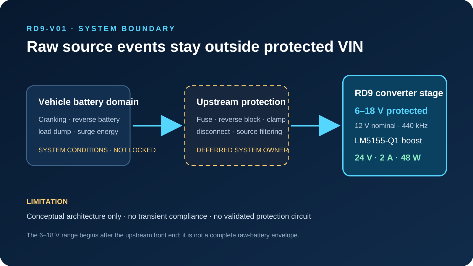
RD9 generates a 24 V auxiliary rail from a protected 12 V battery-domain node for start-stop-aware automotive electronics. It defines the converter stage and evidence still needed; it does not prescribe the end load, raw battery front end, vehicle-level safety concept or qualification plan.
- Domain
- Automotive power electronics
- Application
- 24 V auxiliary-rail generation
- Design state
- CALCULATED_DESIGN
- Isolation
- None · non-isolated
03
Protected input and responsibility boundary
The conversion stage starts at a protected 6–18 V node, with 12 V nominal. The raw vehicle source is outside that envelope. Reverse-battery blocking, load-dump and surge-energy control, fusing, disconnect behavior and source filtering belong to the upstream automotive front end.
| Quantity | Locked value | Evidence class | Interpretation |
|---|---|---|---|
| Nominal converter input | 12 V | PROJECT_REQUIREMENT | Protected battery-domain node |
| Normal converter input | 6–18 V | PROJECT_REQUIREMENT | Continuous calculation range |
| Raw battery transients | Not locked | DEFERRED | Upstream protection owns containment |
| Controller operating capability | 3.5–45 V | OFFICIAL_DEVICE_FACT | Device fact, not system transient proof |
04
Official vendor context and device identity
TI identifies LM5155-Q1 as an active automotive-qualified peak-current-mode controller for non-synchronous boost, SEPIC and flyback use. The selected orderable is LM5155QDSSRQ1 in WSON/DSS-12 tape-and-reel. TI's LM5155EVM-BST standard configuration is 6–18 V input, 24 V at 2 A and 440 kHz; those values are vendor EVM context, not Hengshun measurements.
05
Boost power architecture
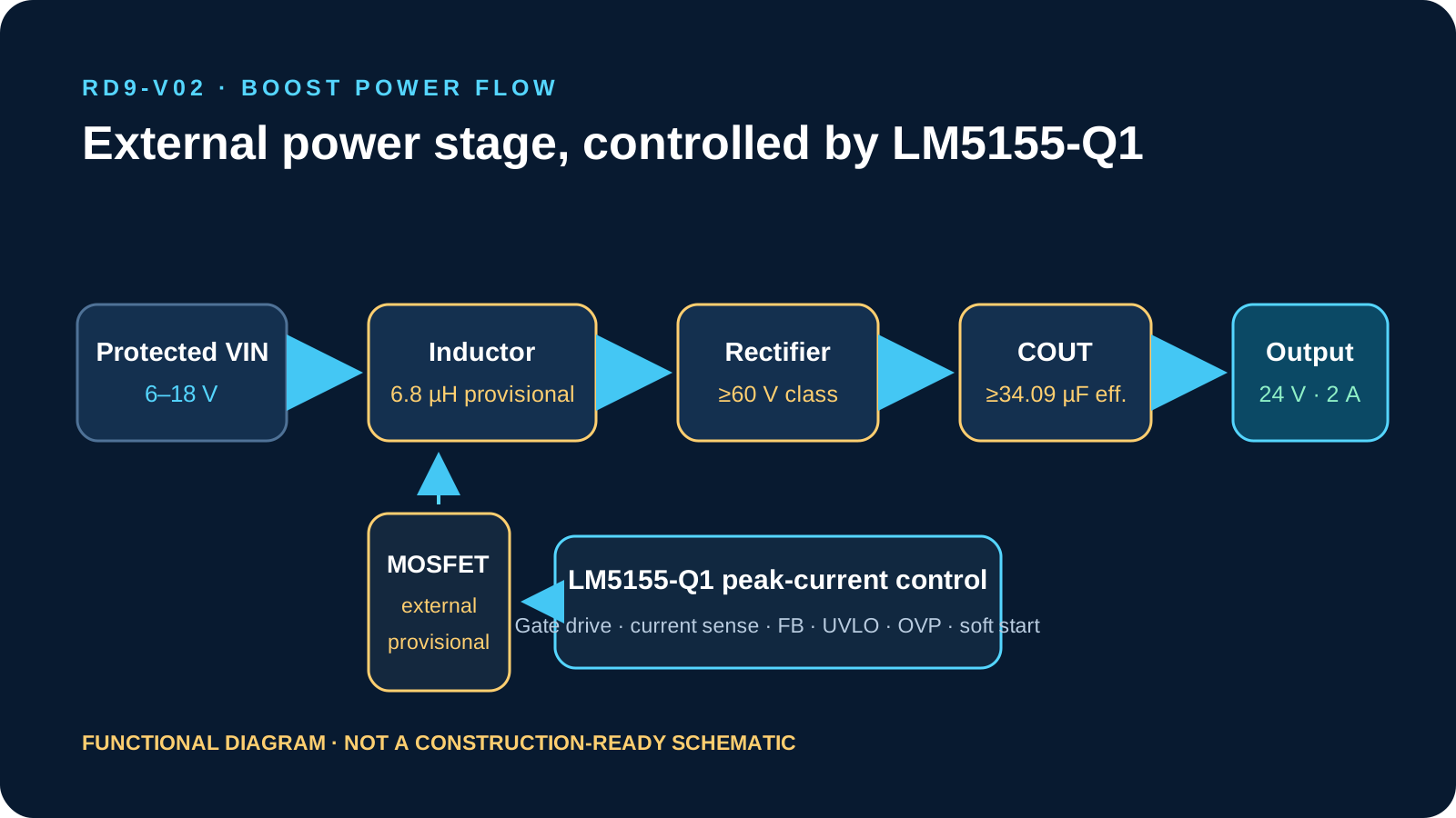
Protected VIN feeds the provisional 6.8 µH inductor. LM5155-Q1 drives an external N-channel MOSFET, the rectifier transfers inductor energy to the output while the switch is off, and the output capacitor supports the 24 V rail. Current sense, feedback, UVLO, OVP, soft-start and compensation networks close the control and protection functions.
06
Fifteen reproducible calculation screens
The table preserves all Stage A calculations. Results are analytical screens rather than simulation or physical evidence; equations omit the limitations stated in each row.
| ID | Inputs / equation | Result | Status and limitation |
|---|---|---|---|
| CALC-01 | 24 V × 2 A | 48 W output | CALCULATED_RESULT |
| CALC-02 | 48 W / 0.90 | 53.33 W assumed input | 90% provisional efficiency |
| CALC-03 | 53.333 W / 6 V | 8.89 A average input | Low-line full-load screen |
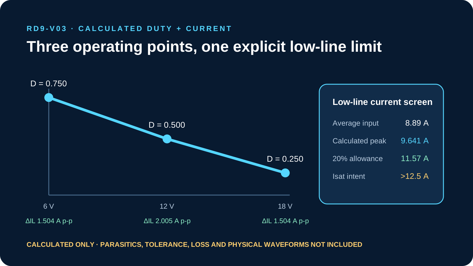
| CALC-04 | D = 1 − VIN/24 V | 0.750 / 0.500 / 0.250 | Ideal at 6 / 12 / 18 V |
| CALC-05 | VIN·D / (6.8 µH·440 kHz) | 1.504 / 2.005 / 1.504 A p-p | Provisional inductance |
| CALC-06 | 8.889 A + 1.504 A / 2 | 9.641 A peak | Ideal low-line current |
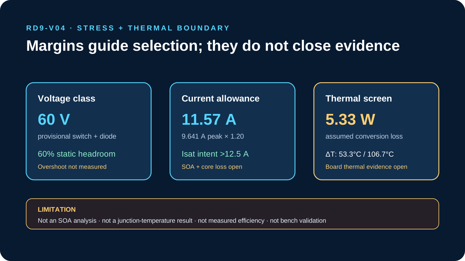
| CALC-07 | 9.641 A × 1.20 | 11.57 A design allowance | Inductor Isat intent >12.5 A |
| CALC-08 | (60 V − 24 V) / 60 V | 60% static rating headroom | Provisional rating; overshoot excluded |
| CALC-09 | 2 A·0.75 / (440 kHz·0.1 V) | 34.09 µF effective minimum | Ideal ripple; ESR/transient excluded |
| CALC-10 | 1.504 A / (8·440 kHz·100 µF) | 4.27 mV p-p | Ideal input ripple; ESR/wiring excluded |
| CALC-11 | 10 kΩ·(24 V / 1 V − 1) | 230 kΩ upper divider | Provisional; tolerance review required |
| CALC-12 | 48 W·(1/0.90 − 1) | 5.33 W loss budget | Assumption, not measured efficiency |
| CALC-13 | 5.333 W·10 or 20°C/W | 53.3°C / 106.7°C rise | Illustrative thermal sensitivity only |
| CALC-14 | 45 V − 18 V | 27 V controller headroom | Not raw-battery transient proof |
| CALC-15 | 0.5·100 µF·24² | 0.0288 J stored energy | Provisional capacitance |
07
Magnetics and current-stress screen
With the provisional 6.8 µH value, the 12 V point creates the largest ideal ripple while the 6 V point creates the largest average and peak input current. The 11.57 A allowance and greater-than-12.5 A saturation intent do not replace core-loss, DCR, tolerance, temperature-rise or saturation-curve review.
08
Capacitors, feedback and startup
The output requires at least 34.09 µF effective capacitance under the ideal 100 mV screen; a provisional 100 µF bulk value plus ceramics remains subject to derating and stability review. A 10 kΩ lower and 230 kΩ upper divider is a mathematical 24 V starting point. Soft-start capacitance, compensation and exact tolerances remain open.
09
Voltage, loss and thermal planning screen
A provisional 60 V switch and rectifier class has 60% headroom relative to the ideal 24 V static stress, but switching overshoot and fault stress are not known. The 5.33 W loss budget and 53.3°C / 106.7°C illustrative rises show why device loss allocation, PCB copper, airflow and physical thermal characterization remain mandatory.
10
Protection, fault and recovery ownership
The controller provides programmable line UVLO, constant peak current limiting, output overvoltage protection, adjustable soft-start, PGOOD and thermal shutdown at device level. Exact thresholds, sense resistance, overload timing, short-circuit response and recovery policy are provisional or deferred; the upstream front end owns raw-source faults.
11
Critical BOM maturity
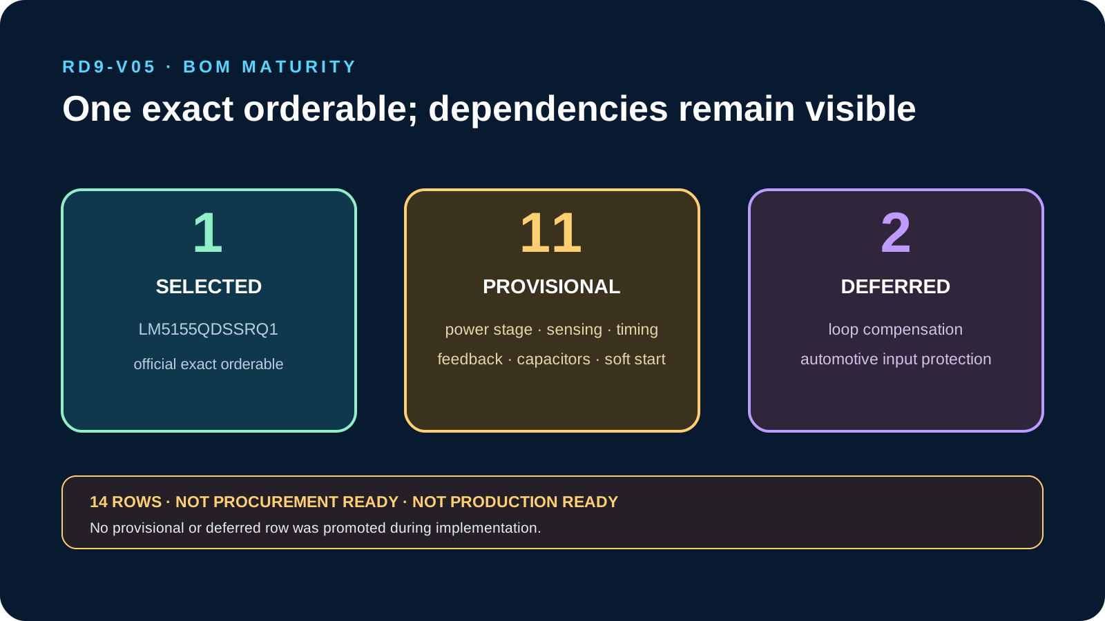
The Stage A maturity split is preserved exactly. LM5155QDSSRQ1 is selected; eleven circuit dependencies remain provisional and two system/control dependencies remain deferred. Blank MPN cells are intentional and prevent unsupported procurement claims.
| ID | Function | Candidate / requirement | Status | Open dependency |
|---|---|---|---|---|
| BOM-01 | Boost controller | LM5155QDSSRQ1 · Texas Instruments | SELECTED | Footprint and assembly-rule confirmation |
| BOM-02 | External MOSFET | N-channel · provisional ≥60 V | PROVISIONAL | Loss, gate charge, SOA and thermal selection |
| BOM-03 | Boost rectifier | Provisional ≥60 V / ≥10 A class | PROVISIONAL | Leakage, loss, thermal and surge review |
| BOM-04 | Boost inductor | 6.8 µH screen · Isat >12.5 A | PROVISIONAL | Core loss, DCR, tolerance and height |
| BOM-05 | Current sense | Low-inductance network | PROVISIONAL | Exact resistance, pulse power and Kelvin layout |
| BOM-06 | Frequency setting | 49.9 kΩ example | PROVISIONAL | Grade, tolerance and frequency equation |
| BOM-07 | Feedback upper | 230 kΩ mathematical screen | PROVISIONAL | Bias, OVP interaction and tolerance |
| BOM-08 | Feedback lower | 10.0 kΩ mathematical screen | PROVISIONAL | Equation and tolerance stack |
| BOM-09 | Input capacitance | 100 µF screen plus ceramics | PROVISIONAL | RMS current, bias and source interaction |
| BOM-10 | Output capacitance | ≥34.09 µF effective; 100 µF start | PROVISIONAL | ESR, bias, transient and stability |
| BOM-11 | Sense filter | 100 Ω / 100 pF vendor-example start | PROVISIONAL | Noise and leading-edge behavior |
| BOM-12 | Soft start | Capacitor value TBD | PROVISIONAL | Ramp and load interaction |
| BOM-13 | Loop compensation | Network TBD | DEFERRED | Final L/C/ESR and loop evidence |
| BOM-14 | Automotive input protection | Front-end architecture TBD | DEFERRED | Transient standard, energy and protected-node guarantee |
12
Planned bench validation
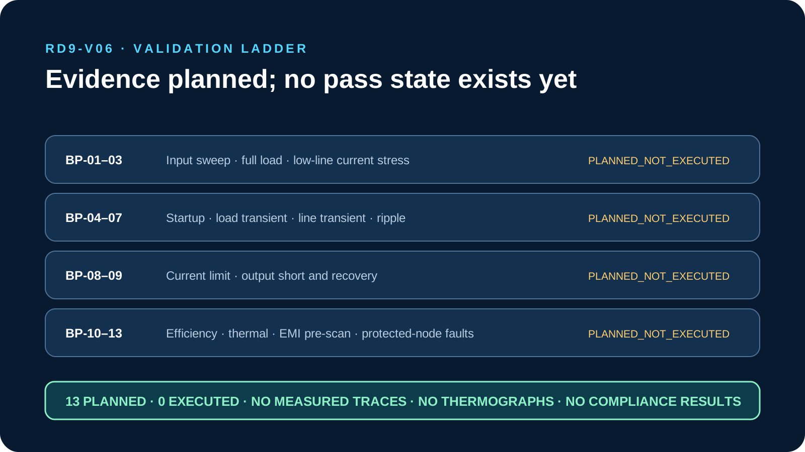
The plan contains thirteen future evidence items and zero executed items. Acceptance intent is recorded to make later testing auditable; no item has a pass or fail result.
- PLANNED_NOT_EXECUTED — BP-01 Input operating sweep: use a programmable DC source, electronic load and DMMs to check the future 24 V tolerance band across 6–18 V.
- PLANNED_NOT_EXECUTED — BP-02 Full-load operation: sweep 0–2 A at 12 V input and observe regulation and protection behavior.
- PLANNED_NOT_EXECUTED — BP-03 Low-line current stress: capture peak and RMS current at 6 V input and 2 A output with a current probe.
- PLANNED_NOT_EXECUTED — BP-04 Startup and shutdown: inspect soft-start and overshoot at 6 V, 12 V and 18 V input.
- PLANNED_NOT_EXECUTED — BP-05 Load transient: apply defined load steps and compare deviation and recovery with future acceptance limits.
- PLANNED_NOT_EXECUTED — BP-06 Line transient: apply controlled 6 V, 12 V and 18 V transitions and record regulation behavior.
- PLANNED_NOT_EXECUTED — BP-07 Output ripple: use a bandwidth-defined probe and short ground spring to quantify ripple and switching artifacts.
- PLANNED_NOT_EXECUTED — BP-08 Current-limit behavior: apply a controlled overload and verify the final sense network and component stress.
- PLANNED_NOT_EXECUTED — BP-09 Output short behavior: use a current-limited source and short fixture to establish the safe recovery policy.
- PLANNED_NOT_EXECUTED — BP-10 Efficiency map: collect Hengshun-owned results at 6 V, 12 V and 18 V with calibrated power meters.
- PLANNED_NOT_EXECUTED — BP-11 Thermal characterization: stabilize ambient conditions and inspect controller, MOSFET, diode, inductor and capacitor temperatures.
- PLANNED_NOT_EXECUTED — BP-12 Conducted and radiated pre-scan: use a defined LISN and pre-scan setup for engineering diagnostics, not a compliance claim.
- PLANNED_NOT_EXECUTED — BP-13 Protected-node fault injection: verify that an approved upstream front end keeps the converter node inside the locked envelope.
13
Visual evidence boundary
Six local semantic visuals explain the protected-input boundary, boost architecture, calculated duty/current screen, stress and thermal screen, BOM maturity and future validation ladder. They contain no stock imagery, fabricated oscilloscope traces, thermographs or measured curves.
- RD9-V01 — System boundary · conceptual architecture only
- RD9-V02 — Boost power flow · functional diagram, not a released schematic
- RD9-V03 — Duty and current · calculated markers only
- RD9-V04 — Stress and thermal · planning screen, not SOA or temperature evidence
- RD9-V05 — BOM maturity · status map, not procurement readiness
- RD9-V06 — Validation ladder · all thirteen items planned and not executed
14
Official sources
The engineering identity and vendor context use first-party Texas Instruments sources. The product page and datasheet govern device facts; the EVM page and guide govern vendor-example context; the application note supports the design method; and the packaging lookup supports the exact orderable identity.
15
Related public engineering context
The reviewed relationship set connects this design to Automotive, ECU Power, DC-DC Power Conversion, Power Protection, the automotive input-transient guide and two adjacent automotive reference designs. The buck-selection guide remains discovery-only, and no LM5155-Q1 component guide is invented.