01
Validation status and limitations
This is a calculated English-only publication candidate, not a released schematic or qualified product. No Hengshun prototype, waveform, efficiency map, temperature map, clamp capture, isolation evaluation, EMI result, surge result or compliance report exists. TI EVM results remain manufacturer reference evidence and are not transferred to this implementation.
Evidence boundary
- Bench validation: NOT EXECUTED
- Thermal characterization: NOT EXECUTED
- EMI, surge and compliance testing: NOT EXECUTED
- Production and field qualification: NOT EXECUTED
02
Design intent and application boundary
RD6 supplies an isolated 15 W-class auxiliary rail from a protected industrial 48 V distribution bus. The conversion stage begins after system-level source protection; it is intended to inform architecture and component review where galvanic isolation is required, not to define a universal industrial interface.
- Application
- Industrial auxiliary power
- Topology
- Primary-side-regulated isolated flyback
- Design state
- CALCULATED_DESIGN
03
Official EVM envelope versus Hengshun target
Texas Instruments documents LM5185EVM-SIO for 20–60 V input, 16.4 V output and a 1 A rated load with a 350 kHz maximum switching frequency. Hengshun uses the same reference envelope but locks 0.9 A and 14.76 W as its calculated continuous target to create operating-current margin. TI did not validate this Hengshun target.
| Attribute | Official TI reference | Hengshun RD6 | Evidence class |
|---|---|---|---|
| Input | 20–60 V | 20–60 V protected node | OFFICIAL_SOURCE_FACT / PROJECT_BOUNDARY |
| Output voltage | 16.4 V | 16.4 V isolated | OFFICIAL_SOURCE_FACT |
| Output current | 1 A rated load | 0.9 A continuous target | CALCULATED_DESIGN_VALUE |
| Output power | 16.4 W nominal rating | 14.76 W calculated | CALCULATED_DESIGN_VALUE |
04
System power tree and isolation boundary
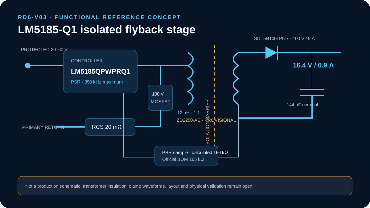
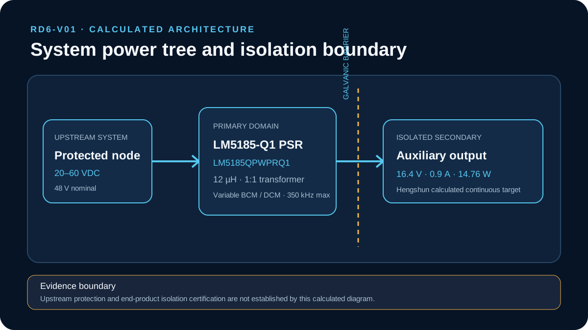
Protected 20–60 V node → input filter and bulk network → LM5185-Q1 PSR controller with external MOSFET → 12 µH 1:1 flyback transformer → 100 V Schottky rectifier and 144 µF nominal output bank → isolated 16.4 V load. Only the transformer crosses the power barrier; the optional barrier capacitor remains provisional.
05
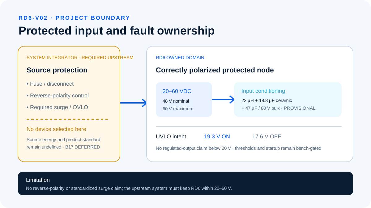
Protected input and fault ownership
RD6 owns operation only at the correctly polarized protected node. The upstream system owns fuse/disconnect, reverse blocking and any surge or overvoltage limiting required to maintain 20–60 V. No front-end TVS, eFuse or surge standard is invented in this design.
06
Startup, UVLO and brownout
The official 200 kΩ / 16.9 kΩ divider targets 19.3 V turn-on and 17.6 V turn-off. A 22 nF soft-start capacitor provides a controlled startup reference, while actual rise time, hysteresis corners, restart delay and output behavior require bench observation.
07
Primary controller identity
The selected controller is LM5185-Q1 and the exact active orderable part is LM5185QPWPRQ1 in a 14-pin PWP HTSSOP package. Its 4.5–100 V controller input range and AEC-Q100 grade 1 device qualification do not qualify the complete converter or isolation system.
08
Flyback architecture and regulation
Primary-side regulation samples the reflected secondary voltage without an optocoupler or auxiliary winding. The calculated feedback value is 166 kΩ; the official standard-value BOM uses 165 kΩ. Output accuracy across line, load, temperature and tolerances remains a physical validation item.
09
Duty cycle and switching frequency
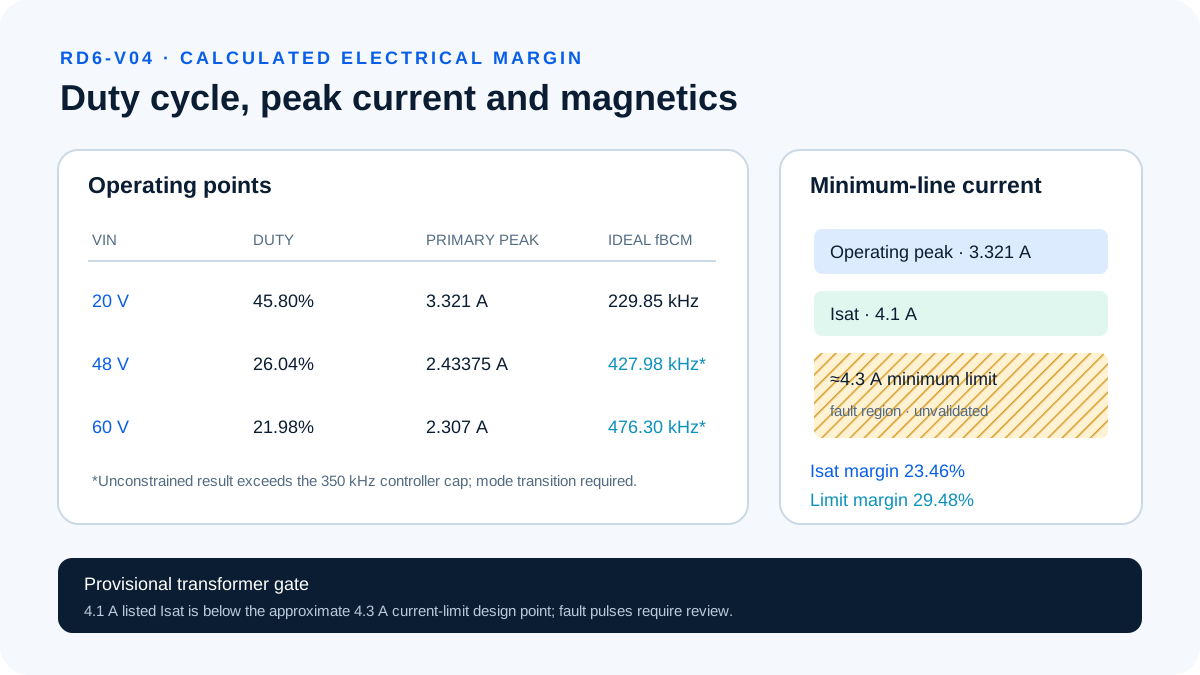
With a 0.5 V diode-drop assumption and 1:1 ratio, calculated duty cycles are 45.80%, 26.04% and 21.98% at 20 V, 48 V and 60 V. Ideal unconstrained BCM frequency is 229.85 kHz at 20 V, 427.98 kHz at 48 V and 476.30 kHz at 60 V; the latter points exceed the 350 kHz controller maximum and enter a controlled mode transition.
10
Transformer and current-limit margin
Calculated primary peaks are 3.321 A at 20 V, 2.43375 A at 48 V and 2.307 A at 60 V. The 4.1 A transformer Isat provides 23.46% operating margin at minimum line, and the approximate 4.3 A minimum current-limit point provides 29.48% margin to normal peak. Because Isat is below that fault design point, ZD2250-AE remains provisional.
11
Switch and rectifier voltage stress
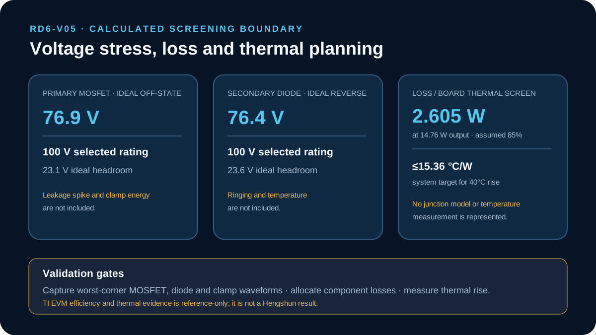
The ideal MOSFET off-state result is 76.9 V and the ideal secondary diode reverse result is 76.4 V. The selected NVMFS021N10MCLT1G and SDT5H100LP5-7 are rated 100 V, but leakage spikes, ringing, clamp energy and temperature are excluded from those ideal calculations and require captured waveforms.
12
Input and output capacitance
The reference input inventory totals 65.8 µF nominal: 18.8 µF ceramic plus 47 µF bulk. The output totals 144 µF nominal: 100 µF electrolytic plus 44 µF ceramic. The 12.45 mV peak-to-peak ideal capacitive ripple screen excludes ESR, switching spikes, bias, aging and placement effects.
13
Feedback, sensing and clamp networks
The selected 20 mΩ current-sense shunt requires Kelvin routing. The 165 kΩ feedback BOM choice is the nearest official standard value to the 166 kΩ calculation. Primary clamp and secondary zener parts follow the EVM concept, while repetitive energy and protection accuracy remain uncharacterized.
14
Loss and thermal planning screen
At the project-defined 85% efficiency screen, calculated input power is 17.365 W and loss is 2.605 W. A 40°C board-level rise planning target implies a system thermal path of no more than 15.36°C/W. Component loss allocation, junction temperatures, airflow and enclosure effects have not been established.
15
Critical BOM maturity
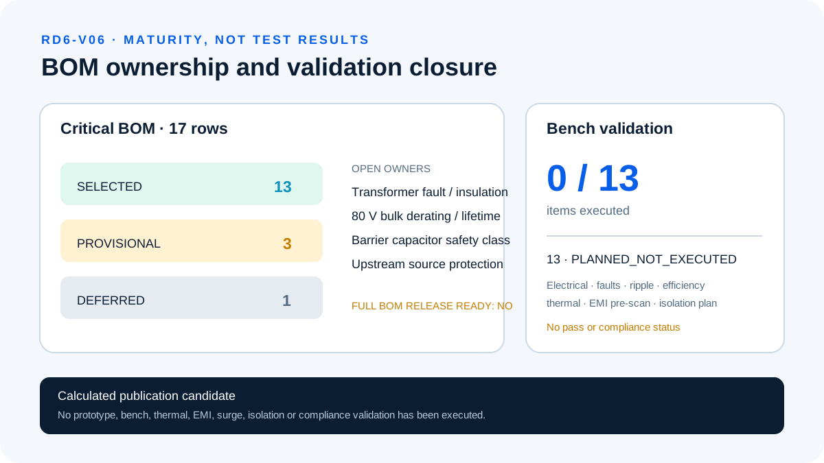
Every critical row is visible below. Three parts remain provisional and one system function remains deferred; none is silently promoted by publication.
| ID | Function | Exact part | Status | Open evidence |
|---|---|---|---|---|
| B01 | PSR controller | LM5185QPWPRQ1 | SELECTED | Availability recheck |
| B02 | Flyback transformer | ZD2250-AE | PROVISIONAL | Fault Isat and insulation system |
| B03 | Primary MOSFET | NVMFS021N10MCLT1G | SELECTED | Drain spike / clamp energy |
| B04 | Secondary rectifier | SDT5H100LP5-7 | SELECTED | Reverse spike / temperature |
| B05 | Current-sense shunt | PRL1632-R020-F-T1 | SELECTED | Pulse and layout review |
| B06 | Leakage-clamp zener | SMBJ5362B-TP | SELECTED | Repetitive clamp energy |
| B07 | Leakage-clamp diode | ACDBMT1100-HF | SELECTED | Spike current / temperature |
| B08 | Secondary protection zener | SMAZ18-13-F | SELECTED | Fault-energy coordination |
| B09 | Input filter inductor | XAL5050-223MEB | SELECTED | Conducted-noise verification |
| B10 | Input ceramic bank | C3225X7S2A475K200AB | SELECTED | DC-bias capacitance |
| B11 | Input bulk capacitor | 865081757008 | PROVISIONAL | 80 V derating, ripple and life |
| B12 | Output bulk capacitor | EEE-FK1E101XP | SELECTED | Ripple lifetime |
| B13 | Output ceramic bank | GRM32ER71E226KE15L | SELECTED | DC-bias capacitance |
| B14 | Feedback resistor | CRCW0603165KFKEA | SELECTED | Output tolerance |
| B15 | UVLO divider | RC0603FR-07200KL + RC0603FR-0716K9L | SELECTED | Threshold corners |
| B16 | Barrier capacitor | 202R18W102KV4E | PROVISIONAL | Safety class and common-mode current |
| B17 | Upstream protection | TBD | DEFERRED | Source fault energy and transient standard |
16
BOM convergence gates
Before hardware release, choose a transformer path that closes fault-current and insulation requirements, review or replace the 80 V input bulk capacitor for the 60 V node, classify the optional barrier capacitor against the end-product standard, and define upstream protection from the real source-energy profile.
17
Layout and isolation priorities
Use compact switching and clamp loops, Kelvin sense routing, controlled primary and secondary return paths, and a clearly declared isolation keep-out. Creepage, clearance, working voltage, pollution degree, material group and transformer insulation construction depend on the end-product standard and are not yet locked.
18
Planned bench validation
The thirteen gates below are plans only. Zero items have been executed, and the matrix does not provide pass evidence.
- PLANNED_NOT_EXECUTED — BP01 current-limited bring-up at 20 / 48 / 60 V
- PLANNED_NOT_EXECUTED — BP02 static line/load regulation from no-load through 0.9 A
- PLANNED_NOT_EXECUTED — BP03 10↔90% and application-specific load-step response
- PLANNED_NOT_EXECUTED — BP04 startup, soft-start, 19.3 V turn-on and 17.6 V turn-off recovery
- PLANNED_NOT_EXECUTED — BP05 current-limit, transformer, short-circuit and hiccup recovery
- PLANNED_NOT_EXECUTED — BP06 controlled protected-node excursions to 20 V and 60 V
- PLANNED_NOT_EXECUTED — BP07 upstream reverse-polarity interface review
- PLANNED_NOT_EXECUTED — BP08 independent line/load efficiency map
- PLANNED_NOT_EXECUTED — BP09 output ripple and noise with declared probe method
- PLANNED_NOT_EXECUTED — BP10 switch, diode and clamp waveform stress captures
- PLANNED_NOT_EXECUTED — BP11 component thermal characterization at ambient corners
- PLANNED_NOT_EXECUTED — BP12 conducted and radiated EMI pre-scan
- PLANNED_NOT_EXECUTED — BP13 isolation construction, creepage, clearance and dielectric plan
19
Visual evidence boundary
Six local engineering diagrams expose the architecture, ownership boundaries, calculations and maturity. They are explanatory calculated/reference visuals, not photographs, PCB renders, oscilloscope traces, thermal images or certification marks.
| Visual ID | Purpose | Locked content | Limitation |
|---|---|---|---|
| RD6-V01 | System power tree | 20–60 V → isolated 16.4 V / 0.9 A | Calculated architecture |
| RD6-V02 | Input ownership | 22 µH; 65.8 µF; 19.3 / 17.6 V | Upstream protection required |
| RD6-V03 | Flyback stage | LM5185QPWPRQ1; 12 µH; 20 mΩ | Reference schematic concept |
| RD6-V04 | Magnetic margin | Duty / peak / 23.46% / 29.48% | Fault region unvalidated |
| RD6-V05 | Stress and loss | 76.9 V; 76.4 V; 2.605 W; 15.36°C/W | Calculated screen only |
| RD6-V06 | Maturity map | 13 / 3 / 1 BOM; 0 of 13 tests | Not a physical-test dashboard |
20
Official evidence and related engineering context
These official sources support controller identity, design equations, EVM envelope and reference BOM. The related LM5161-Q1 guide is alternative Fly-Buck context only; LM5161-Q1 is not the controller used by RD6.