01
Validation status and limitations
This English-only page is a calculated publication candidate, not a released schematic or qualified product. It contains no Hengshun prototype data, waveform capture, efficiency measurement, temperature map, EMI result, surge result, isolation-system evaluation or compliance report. Manufacturer EVM results remain official third-party context and are not transferred to this implementation.
Evidence boundary
- Bench validation: NOT EXECUTED
- Thermal characterization: NOT EXECUTED
- EMI, surge and compliance testing: NOT EXECUTED
- System isolation and production qualification: NOT EXECUTED
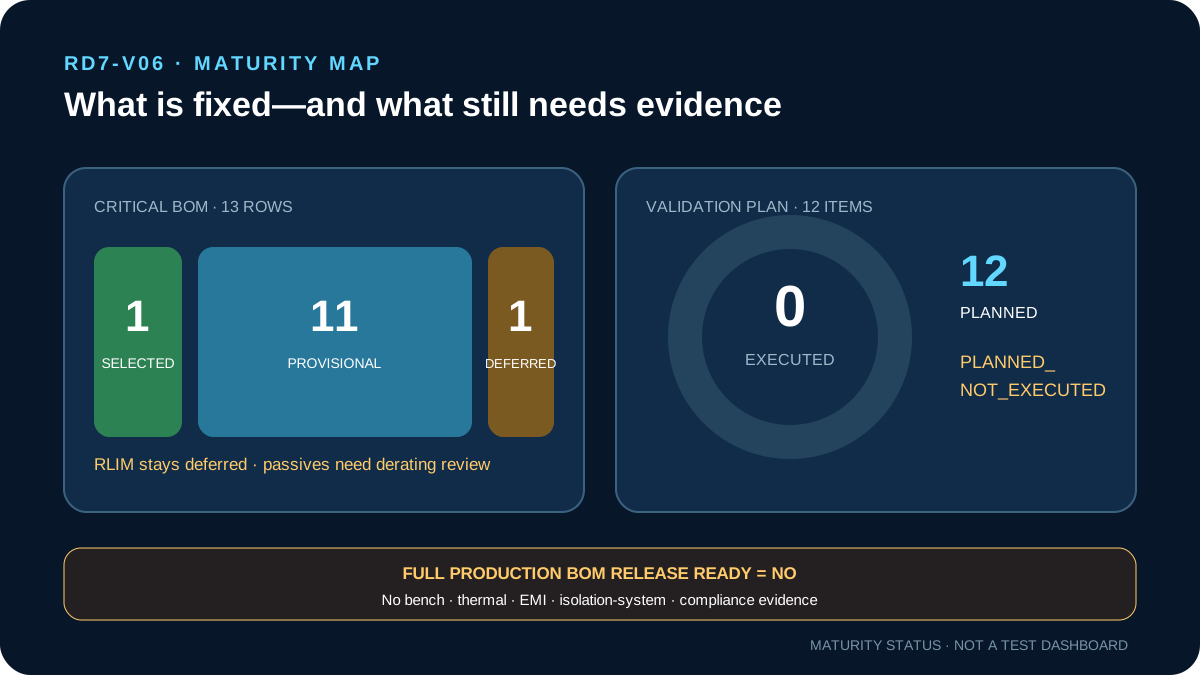
- Full production BOM release readiness: NO
02
Design intent and end application
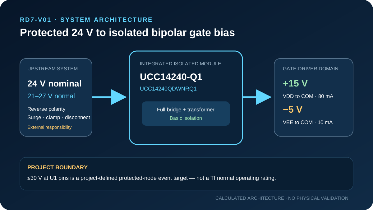
RD7 provides compact isolated bipolar bias power for a SiC or IGBT gate-driver domain in industrial motor drives, robot servo inverters and related power-conversion equipment. It begins at a regulated and protected 24 V auxiliary node and ends at the driver-bias rails; it does not define the upstream distribution bus or the gate driver itself.
- Application
- Industrial gate-driver bias
- Topology
- Integrated-transformer isolated full bridge
- Design state
- CALCULATED_DESIGN
03
Input envelope and protected-node ownership
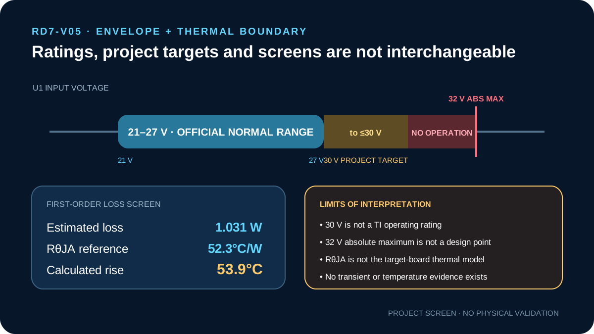
The official normal UCC14240-Q1 input range is 21–27 V, with 24 V nominal. A brief ≤30 V value at U1 pins is only a project-defined protected-node event target. It is not TI's normal operating rating, and the 32 V absolute maximum is not a design operating point. Reverse polarity, surge limiting and disconnect remain upstream system functions.
| Quantity | Locked value | Evidence class | Interpretation |
|---|---|---|---|
| Nominal input | 24 VDC | PROJECT_DESIGN_POINT | Protected auxiliary rail |
| Normal input | 21–27 VDC | OFFICIAL_DEVICE_FACT | Required operating range |
| Protected-node event | ≤30 V | PROJECT_DEFINED_ASSUMPTION | Short event target; normal operation ends above 27 V |
| Absolute maximum | 32 V | OFFICIAL_DEVICE_FACT | Stress ceiling, not an operating rating |
04
Integrated isolated-bias architecture
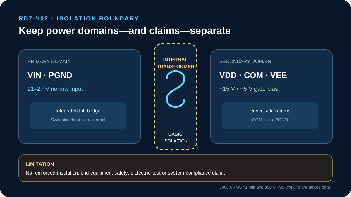
UCC14240QDWNRQ1 integrates its transformer, full-bridge switching stage and isolated power transfer. The primary VIN/PGND domain remains separate from the VDD/COM/VEE gate-driver domain. Integration removes an external magnetics calculation but does not remove PCB keepout, thermal, common-mode, load-balance or system-safety review.
05
Basic-isolation boundary
Device documentation provides basic-isolation evidence including 3000 VRMS for one minute and 850 VRMS working-voltage data. RD7 claims basic or functional component-level isolation only. Reinforced insulation, end-equipment creepage and clearance, altitude, pollution degree, dielectric test planning and system compliance remain outside this publication candidate.
06
Dual-output regulation
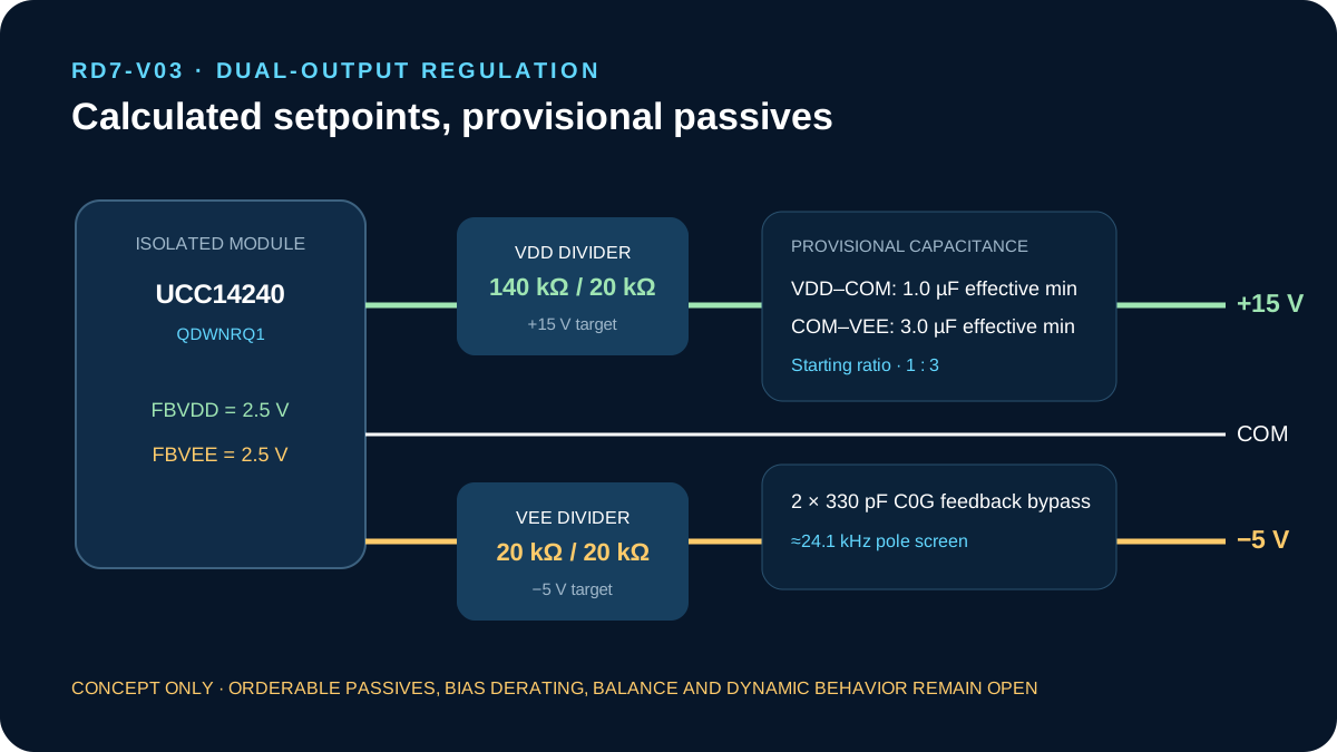
The calculated feedback network uses the 2.5 V references. A 140 kΩ / 20 kΩ VDD divider targets +15 V, while a 20 kΩ / 20 kΩ VEE divider targets -5 V relative to COM. With a ±0.5% feedback-reference screen, the positive rail spans 14.675–15.325 V before external resistor tolerance and loading. These are calculated setpoints, not measured accuracy results.
07
Load and power budget
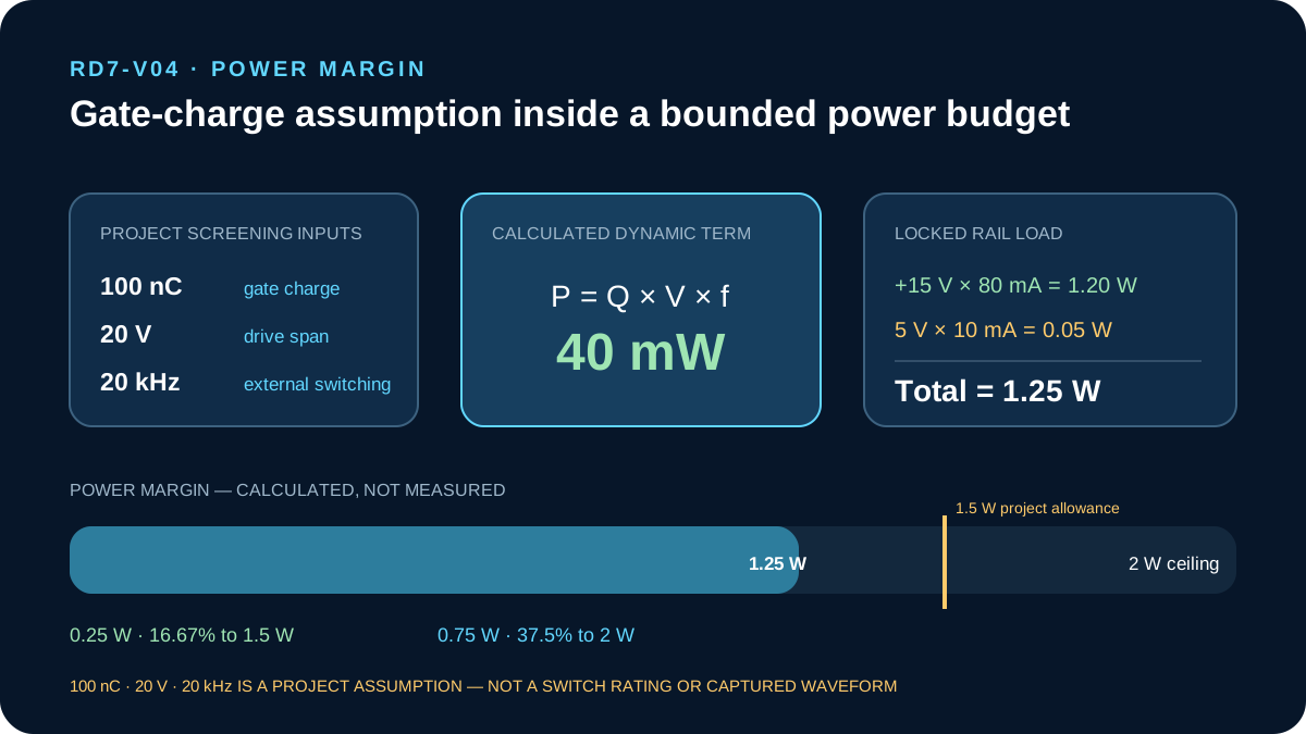
The locked simultaneous rail load is 80 mA at +15 V and 10 mA at -5 V, yielding 1.20 W plus 0.05 W, or 1.25 W total. That leaves 0.25 W or 16.67% to a 1.5 W project planning allowance and 0.75 W or 37.5% to the device's 2 W ceiling. Dynamic gate-driver demand and quiescent current remain application inputs.
08
Gate-charge screening assumption
For planning only, 100 nC switched across a 20 V span at 20 kHz calculates 40 mW of dynamic gate-drive power. The value is an external project assumption used to size local energy storage; it is not a UCC14240-Q1 rating, a selected power-switch claim or a captured load waveform.
09
Capacitor partition and feedback filtering
The starting network uses 10 µF plus 0.1 µF at VIN, 2.2 µF plus 0.1 µF across VDD-to-VEE, and provisional effective branch values of 1.0 µF positive and 3.0 µF negative. A 330 pF capacitor across each 20 kΩ lower feedback resistor produces an approximate 24.1 kHz pole screen. Bias derating, balance and dynamic stability remain open.
10
Startup, brownout and fault recovery
The host must hold gate PWM inactive until PG and the system supervisor both permit operation. The 16 ms watchdog is an official protection behavior; no fixed startup guarantee is published. Brownout, overload or undervoltage latch-off requires fault removal and a controlled ENA or VIN reset before PWM returns.
11
Loss and thermal planning screen
Linear scaling from the referenced 2 W loss condition gives a 1.031 W device-loss estimate at 1.25 W output. Applying 52.3°C/W produces a 53.9°C first-order junction-rise screen and an approximate 139°C result at 85°C ambient. This deliberately conservative screen is not efficiency characterization, a junction model or physical thermal evidence.
12
Critical BOM maturity
Every critical row is visible. UCC14240QDWNRQ1 is selected, eleven passive rows remain provisional and RLIM remains deferred. Publication does not promote any unresolved row.
| ID | Function | Part or value | Status | Open evidence |
|---|---|---|---|---|
| B01 | Isolated bias module | UCC14240QDWNRQ1 | SELECTED | System isolation and upstream protection |
| B02 | Input bulk bypass | 10 µF / 50 V X7R | PROVISIONAL | Orderable part and effective capacitance |
| B03 | Input HF bypass | 0.1 µF / 50 V X7R | PROVISIONAL | Orderable part and placement |
| B04 | Total-output bulk | 2.2 µF / 50 V X7R | PROVISIONAL | Orderable part and effective capacitance |
| B05 | Total-output HF bypass | 0.1 µF / 50 V X7R | PROVISIONAL | Orderable part and placement |
| B06 | VDD divider upper | 140 kΩ / 1% | PROVISIONAL | Tolerance stack |
| B07 | VDD divider lower | 20 kΩ / 1% | PROVISIONAL | Tolerance stack |
| B08 | VEE divider upper | 20 kΩ / 1% | PROVISIONAL | Tolerance stack |
| B09 | VEE divider lower | 20 kΩ / 1% | PROVISIONAL | Tolerance stack |
| B10 | Feedback bypass | 2 × 330 pF C0G | PROVISIONAL | Dynamic behavior |
| B11 | Current-limit programming | RLIM TBD | DEFERRED | Driver IQ, tolerance and load balance |
| B12 | Positive local energy | 1.0 µF effective minimum | PROVISIONAL | DC bias and gate interaction |
| B13 | Negative local energy | 3.0 µF effective minimum | PROVISIONAL | DC bias and transient sharing |
13
Open convergence work
Exact passive orderable identities still require voltage, DC-bias, tolerance and temperature review. RLIM remains deferred until actual gate-driver quiescent current, capacitor tolerance and rail-load balance are approved. These two open items do not change the locked device, topology, input envelope, output targets or public claim boundary.
14
Layout and system-integration priorities
Place VIN and PGND bypass parts at the device, keep each secondary return loop compact, preserve the package isolation keepout and route feedback away from switching fields. Coordinate PG and ENA with the real gate driver so PWM cannot begin before both rails are established. Review common-mode current and barrier spacing in the complete assembly.
15
Planned bench validation
All twelve items below are plans only. Zero have been executed and no item provides pass evidence.
- PLANNED_NOT_EXECUTED — BP01 current-limited 24 V bring-up with ENA and PG sequencing
- PLANNED_NOT_EXECUTED — BP02 static +15 V / -5 V regulation at 21 V, 24 V and 27 V
- PLANNED_NOT_EXECUTED — BP03 positive and negative rail load-step balance and recovery
- PLANNED_NOT_EXECUTED — BP04 overload, short-circuit latch-off and controlled reset
- PLANNED_NOT_EXECUTED — BP05 startup, PG timing, brownout and PWM-inhibit behavior
- PLANNED_NOT_EXECUTED — BP06 bounded protected-node events up to the approved ≤30 V project target
- PLANNED_NOT_EXECUTED — BP07 upstream reverse-polarity interface review with U1 unpowered
- PLANNED_NOT_EXECUTED — BP08 module and passive thermal mapping over line, load and ambient
- PLANNED_NOT_EXECUTED — BP09 input/output power and efficiency map with declared conditions
- PLANNED_NOT_EXECUTED — BP10 VDD-COM and COM-VEE ripple and noise with isolated probing
- PLANNED_NOT_EXECUTED — BP11 conducted and radiated EMI pre-scan plus common-mode current
- PLANNED_NOT_EXECUTED — BP12 isolation spacing, dielectric plan and gate-bias interaction review
16
Visual evidence boundary
Six local engineering diagrams expose the architecture, isolation ownership, calculated regulation, gate-power margin, protection and thermal boundary, and maturity state. They are explanatory calculated or reference visuals—not photographs, PCB renders, oscilloscope traces, thermal images or certification evidence.
| Visual ID | Purpose | Locked content | Limitation |
|---|---|---|---|
| RD7-V01 | System architecture | 21–27 V to +15 V / -5 V | Upstream protection remains external |
| RD7-V02 | Isolation boundary | PGND domain to COM domain | Basic isolation only |
| RD7-V03 | Dual-output regulation | 2.5 V references and capacitor partition | Concept, not released schematic |
| RD7-V04 | Power margin | 40 mW assumption and 1.25 W rail load | Calculated values only |
| RD7-V05 | Envelope and thermal | 21–27 V, ≤30 V, 32 V and 53.9°C | No transient or thermal validation |
| RD7-V06 | Maturity | 1 / 11 / 1 BOM and 0 of 12 tests | Not production release evidence |
17
Official evidence and related engineering context
These Texas Instruments sources support device identity, limits, equations and evaluation context. Related Hengshun content provides upstream and topology comparisons only; LM5161-Q1 is not part of the RD7 BOM and no UCC14240-Q1 Component Guide route is asserted.