01
Validation status and claim limits
RD11 is an English-only calculated publication candidate, not a released schematic, measured module or qualified automotive product. The primary IC identity, vendor specifications, project requirements and calculation bundle are reviewable evidence; physical efficiency, standby current, thermal behavior, EMI, fault response and raw-battery protection have not been measured on Hengshun hardware.
Evidence boundary
- Board and bench validation: NOT EXECUTED
- Thermal characterization: NOT EXECUTED
- EMI and compliance testing: NOT EXECUTED
- Measured efficiency, sleep current and transient response: NOT COLLECTED
- Raw-battery surge and reverse-polarity survival: OUTSIDE THE RD11 CONVERTER-NODE BOUNDARY
- Production readiness: NO
02
Project requirements and system boundary
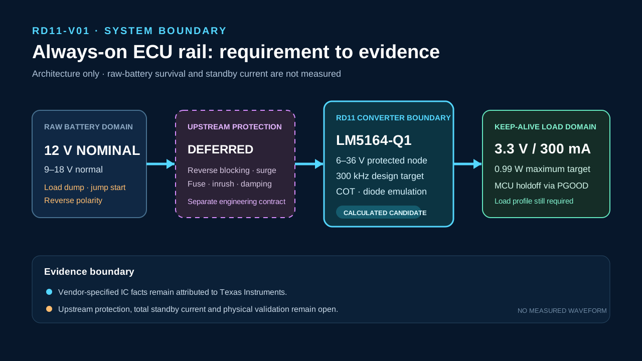
The project requirement is an automotive ECU keep-alive rail supplied from a protected node: 12 V nominal, 9–18 V normal and 6–36 V continuous. RD11 targets one 3.3 V output at up to 300 mA and a nominal 300 kHz switching frequency. An upstream stage owns reverse polarity, load-dump energy, jump-start behavior, inrush, fuse coordination and damping; no event capability is inferred from the converter-node envelope.
- Evidence class
- PROJECT_REQUIREMENTS
- Input
- 12 V nominal · 9–18 V normal · 6–36 V protected node
- Output
- 3.3 V · 0–300 mA · 0.99 W maximum
- Isolation
- None · non-isolated
- Status signal
- Open-drain PGOOD planned; interface remains provisional
03
Vendor-specified device context
Texas Instruments specifies LM5164-Q1 as an automotive 6–100 V, 1 A-class synchronous buck using constant-on-time control with diode-emulation light-load behavior. The datasheet provides a typical 10.5 µA no-load device supply-current context, typical 3 µA shutdown current, 1.2 V feedback reference, 50 ns minimum controllable timing, nominal 3 ms internal soft start, PGOOD and a DDA-package JEDEC RθJA value of 43.4 °C/W. These are device facts under vendor conditions, not Hengshun module measurements or guarantees.
- Evidence class
- VENDOR_SPECIFIED_VALUES
- Selected orderable
- LM5164QDDARQ1
- Device qualification
- AEC-Q100 grade 1 IC only
- Board/system qualification
- Not established
04
Vendor-measured results are not transferred
The LM5164-Q1EVM is an official 300 kHz evaluation context for a 15–100 V input and a 12 V / 1 A output. Its efficiency, waveform, current and temperature results are not transferred to RD11 because the target voltage, load, protected input, layout, passives and system boundary differ. RD11 uses the EVM only as an official device and starting-component reference.
- Evidence class
- VENDOR_MEASURED_RESULTS
- Vendor result used as RD11 performance claim
- 0
05
Synchronous buck implementation concept
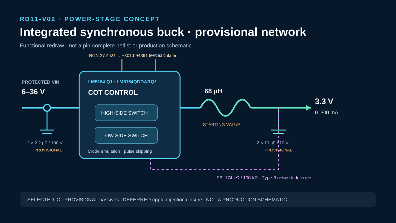
The protected node feeds the integrated LM5164-Q1 high-side and low-side switches. A provisional 68 µH inductor and output-capacitor bank form the 3.3 V rail; the feedback divider senses the output, the RON resistor sets nominal on-time and PGOOD reports regulator status. A Type-3 ripple-injection network is deferred until the final output network and stability review are available. This is a functional architecture, not a pin-complete production netlist.
06
Twenty-one reproducible calculation screens
All twenty-one rows are Hengshun engineering calculations copied from the locked Stage A calculation set. They preserve the equation, declared inputs, units and boundary: ideal first-pass guidance or planning assumptions, never simulated or measured performance.
| ID | Purpose | Equation and inputs | Result | Provenance / boundary |
|---|---|---|---|---|
| C01 | Output-power target | P_OUT = 3.3 V × 0.3 A | 0.990000 W | Project requirement; maximum DC target |
| C02 | Ideal duty at 6 V | D = 3.3 / 6 | 0.550000 ratio | Ideal CCM; losses excluded |
| C03 | Ideal duty at 9 V | D = 3.3 / 9 | 0.366667 ratio | Ideal CCM |
| C04 | Ideal duty at 12 V | D = 3.3 / 12 | 0.275000 ratio | Ideal CCM |
| C05 | Ideal duty at 18 V | D = 3.3 / 18 | 0.183333 ratio | Ideal CCM |
| C06 | Ideal duty at 36 V | D = 3.3 / 36 | 0.091667 ratio | Ideal CCM |
| C07 | Ideal RON for 300 kHz | R_RON(kΩ) = 3.3 × 2500 / 300 | 27.500000 kΩ | Vendor equation; nominal CCM |
| C08 | Frequency with 27.4 kΩ RON | F_SW(kHz) = 3.3 × 2500 / 27.4 | 301.094891 kHz | Provisional resistor; tolerances excluded |
| C09 | Inductance for 40% ripple at 12 V | L = 3.3 × (1−3.3/12) / (300 kHz × 0.12 A) | 66.458333 µH | Ideal heuristic starting point |
| C10 | Ripple at 6 V with 68 µH | ΔI = 3.3 × (1−3.3/6) / (300 kHz × 68 µH) | 0.072794 A_pp | Ideal CCM |
| C11 | Ripple at 12 V with 68 µH | ΔI = 3.3 × (1−3.3/12) / (300 kHz × 68 µH) | 0.117279 A_pp | Ideal CCM |
| C12 | Ripple at 36 V with 68 µH | ΔI = 3.3 × (1−3.3/36) / (300 kHz × 68 µH) | 0.146936 A_pp | Ideal CCM |
| C13 | Worst-envelope peak current | I_PEAK = 0.3 A + 0.146936 A / 2 | 0.373468 A | Startup and fault peaks excluded |
| C14 | Worst-envelope RMS current | I_RMS = sqrt(0.3² + 0.146936²/12) | 0.302984 A_rms | Triangular-ripple screen |
| C15 | Minimum effective COUT | C_OUT = 0.146936 / (8 × 300 kHz × 0.0165 V) | 3.710512 µF_effective | 0.5% target; ESR/ESL and transients excluded |
| C16 | Input-ripple screen at 6 V | ΔV_IN = 0.3 × 0.55 × 0.45 / (4.4 µF × 300 kHz) | 56.250000 mV_pp | Nominal CIN; derating and source impedance excluded |
| C17 | Feedback-divider output | V_OUT = 1.2 × (1 + 174 kΩ / 100 kΩ) | 3.288000 V | Nominal provisional values |
| C18 | Input current at 12 V | I_IN = 0.99 W / (12 V × 0.85) | 97.058824 mA | 85% Hengshun planning assumption |
| C19 | Loss at 12 V full load | P_LOSS = 0.99 × (1/0.85 − 1) | 0.174706 W | Lumped planning estimate |
| C20 | First-order junction-rise screen | ΔT = 0.174706 W × 43.4 °C/W | 7.582235 °C | JEDEC RθJA screen; not a board model |
| C21 | Device-only annual charge context | Q_YEAR = 10.5 µA × 8760 h | 91.980000 mAh_per_year | Typical IC-only context; system contributors excluded |
07
Duty, timing and ripple envelope
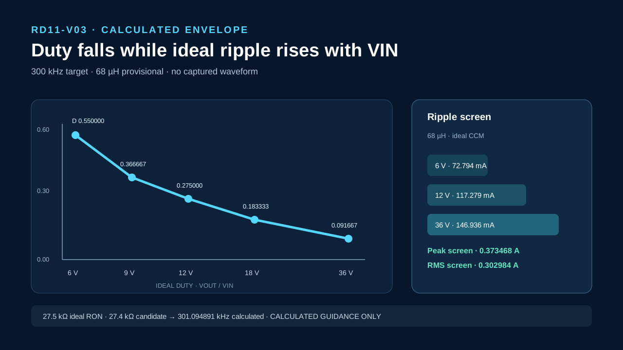
The locked ideal model spans duty ratios from 0.55 at 6 V to 0.091667 at 36 V. With the provisional 68 µH inductor, ripple rises from 72.794 mA p-p to 146.936 mA p-p. The 27.4 kΩ RON candidate calculates approximately 301.094891 kHz. These are calculation markers; actual frequency, pulse skipping, tolerance, current waveforms and minimum-time behavior require bench observation.
08
Standby-current evidence budget
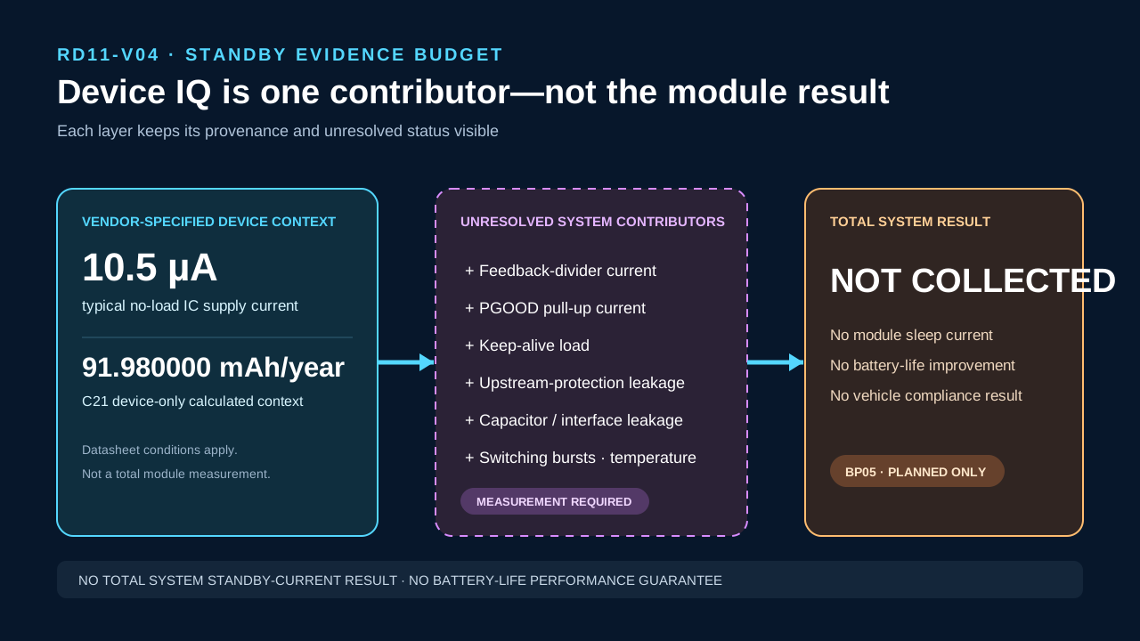
The typical 10.5 µA figure belongs to the LM5164-Q1 device under datasheet conditions. The calculated 91.98 mAh/year value is device-only context. A complete vehicle standby budget must add feedback-divider current, PGOOD pull-up current, keep-alive load, input-protection leakage, capacitor leakage, switching bursts, temperature and tolerance. No total module sleep-current result or battery-life improvement is claimed.
- Evidence class
- VENDOR_SPECIFIED plus HENGSHUN_ENGINEERING_CALCULATION
- Device typical context
- 10.5 µA under datasheet conditions
- Device-only annual context
- 91.980000 mAh/year calculated
- Measured module standby current
- Not collected
09
Critical BOM maturity
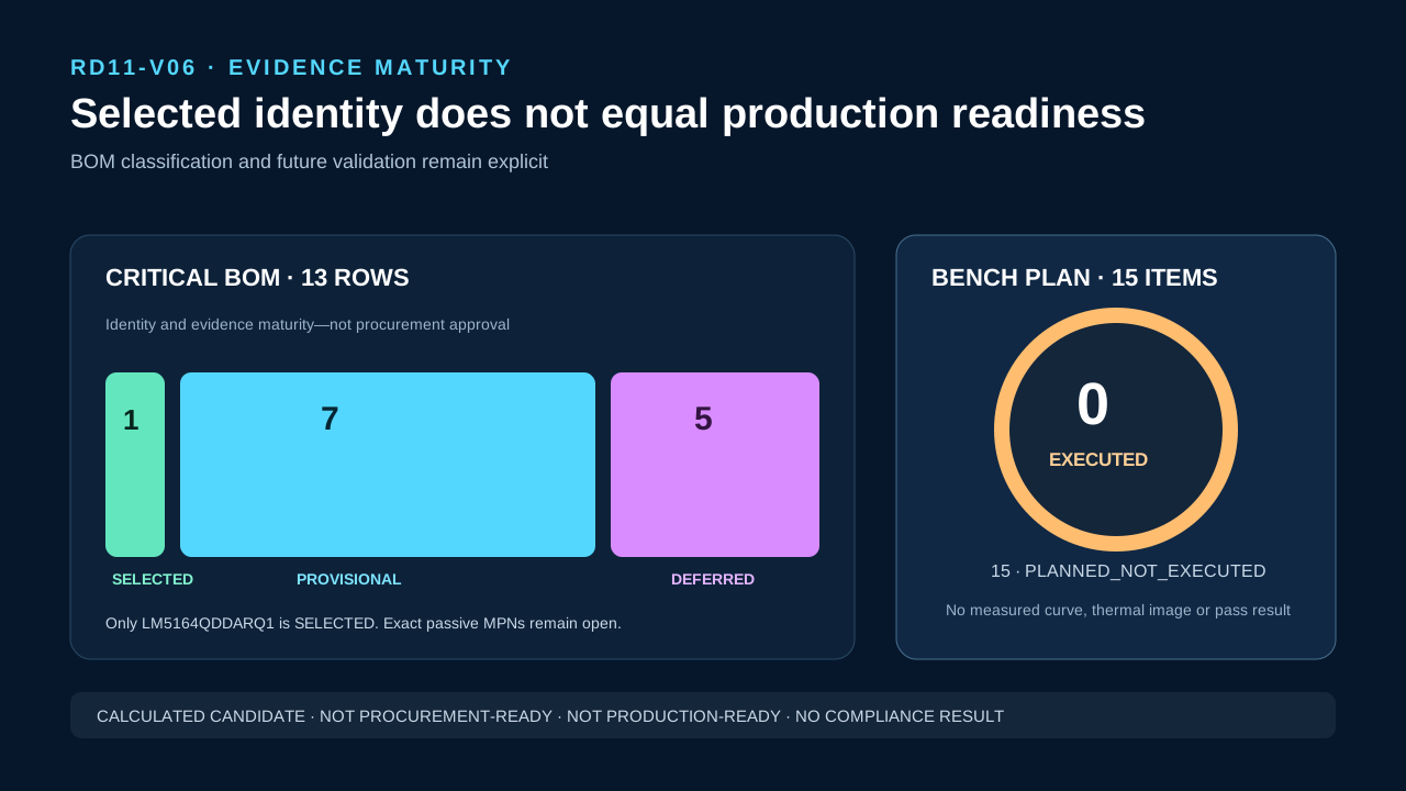
The Stage A maturity split is preserved exactly: one selected row, seven provisional rows and five deferred rows. Selected locks the primary IC identity for this calculated candidate; provisional values need component-level evidence; deferred items depend on later system contracts.
| ID | Function | Candidate or starting value | Status | Open evidence |
|---|---|---|---|---|
| B01 | Primary synchronous buck regulator | LM5164QDDARQ1 | SELECTED | Target-board electrical, thermal, EMC and lifecycle recheck |
| B02 | Power inductor | 68 µH starting value; exact MPN TBD | PROVISIONAL | Tolerance, DCR, saturation, temperature, size and AEC-Q200 evidence |
| B03 | High-frequency input ceramics | 2 × 2.2 µF / 100 V X7R starting network | PROVISIONAL | Package, DC-bias effective C, ripple, tolerance and temperature |
| B04 | Input bulk and damping | Value and technology TBD | DEFERRED | Source impedance, harness, protector and measured ringing |
| B05 | Output capacitor bank | 2 × 10 µF / 10 V X7R nominal starting network | PROVISIONAL | DC-bias, ESR/ESL, transient response and stability network |
| B06 | Bootstrap capacitor | 2.2 nF / 50 V X7R starting value | PROVISIONAL | Package, voltage stress, tolerance and placement |
| B07 | RON timing resistor | 27.4 kΩ 1% starting value | PROVISIONAL | Frequency tolerance, timing margin and measured frequency |
| B08 | Feedback divider | 174 kΩ upper / 100 kΩ lower starting values | PROVISIONAL | Reference/resistor tolerance, temperature and final setpoint |
| B09 | Type-3 ripple-injection network | RA / CA / CB values TBD | DEFERRED | Final COUT/ESR, frequency, VIN, load steps and stability |
| B10 | PGOOD pull-up and interface | Value and logic rail TBD | PROVISIONAL | MCU rail, sink current, thresholds and timing |
| B11 | Automotive input protection | Architecture and parts TBD | DEFERRED | Vehicle pulses, TVS/FET SOA, fuse and safety review |
| B12 | Fuse, connector and harness | System parts TBD | DEFERRED | Harness resistance, connector temperature and service state |
| B13 | PCB copper, thermal path and enclosure | Stack-up and mechanical system TBD | DEFERRED | Copper, airflow, ambient, enclosure, EMC and DFM |
10
Planned bench validation
The Stage A evidence plan contains fifteen future items and zero executed items. Every line describes work that must be performed later under approved conditions; none is a pass result, measured curve, thermal image or compliance conclusion.
- PLANNED_NOT_EXECUTED — BP01 Pre-power inspection: check continuity, resistance, polarity, assembly revision and visible defects before energization.
- PLANNED_NOT_EXECUTED — BP02 Current-limited bring-up at 6, 9, 12, 18 and 36 V while observing VIN, VOUT, input current, startup and PGOOD.
- PLANNED_NOT_EXECUTED — BP03 Protected-node input sweep across 6–36 V at representative 10%, 50% and 100% loads.
- PLANNED_NOT_EXECUTED — BP04 Load sweep from the defined fixture minimum through 300 mA at 9, 12 and 18 V.
- PLANNED_NOT_EXECUTED — BP05 Standby and no-load input-current measurement with a low-current source-measure setup and defined EN/load states.
- PLANNED_NOT_EXECUTED — BP06 Startup, shutdown and PGOOD timing capture for cold start, EN toggle and input ramp conditions.
- PLANNED_NOT_EXECUTED — BP07 Line-regulation measurement over both the 9–18 V normal range and 6–36 V protected-node range.
- PLANNED_NOT_EXECUTED — BP08 Load regulation and transient response for approved load steps within 0–300 mA.
- PLANNED_NOT_EXECUTED — BP09 Ripple and noise measurement with declared bandwidth and a reproducible low-inductance probe setup.
- PLANNED_NOT_EXECUTED — BP10 Switch-node and inductor-current observation at 6, 12 and 36 V across light, mid and full load.
- PLANNED_NOT_EXECUTED — BP11 Efficiency and loss mapping across 6, 9, 12, 18 and 36 V with measurement uncertainty.
- PLANNED_NOT_EXECUTED — BP12 Thermal characterization at selected worst-case line/load points and thermal steady state.
- PLANNED_NOT_EXECUTED — BP13 Current-limit, short-circuit and recovery behavior under an approved bounded safety procedure.
- PLANNED_NOT_EXECUTED — BP14 Interaction with the separately engineered upstream protection stage for a later authorized event set.
- PLANNED_NOT_EXECUTED — BP15 Exploratory EMI pre-scan for engineering discovery only, without a compliance conclusion.
11
Six original technical visuals
Six local code-native SVGs explain the system boundary, synchronous buck concept, calculated envelope, standby-current evidence budget, layout priorities and evidence maturity. They use no remote resources or vendor-diagram copies and contain no fabricated waveform, thermograph, efficiency curve or compliance result.
- RD11-V01 — Always-on ECU system boundary · architecture only
- RD11-V02 — Synchronous buck power-stage concept · not a production schematic
- RD11-V03 — Duty, timing and ripple envelope · calculated guidance only
- RD11-V04 — Standby-current evidence budget · no total system result
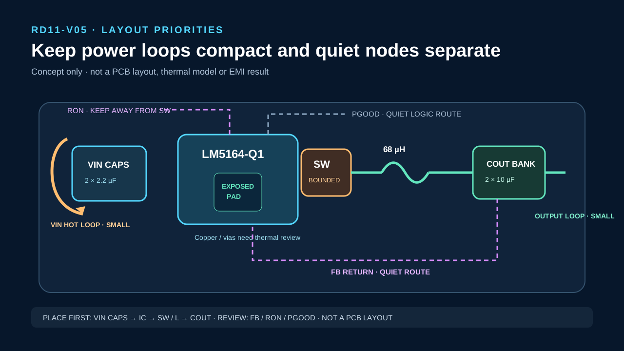
- RD11-V05 — Hot-loop and quiet-node priorities · not a PCB layout or EMI result
- RD11-V06 — BOM and validation maturity · not production readiness
12
Layout and implementation priorities
Place the high-frequency input ceramics across VIN and ground with the smallest practical loop, keep SW copper bounded, and connect the inductor and output ceramics with short high-current paths. Keep feedback, RON and PGOOD away from switch-node coupling and provide an exposed-pad copper path consistent with the later thermal plan. The visual communicates priorities only and is not a manufacturable layout.
13
Relationship implementation plan
Eight reviewed links connect RD11 to existing solution, application, reference-design, guide and conversion surfaces. The absent LM5164-Q1 Component Guide remains explicit plain text, a future always-on budgeting guide remains discovery-only, and localized editions remain deferred without placeholder routes.
| ID | Target | Public action | Status |
|---|---|---|---|
| R01 | DC-DC Power Conversion | /solutions/dc-dc-converters/ | RESOLVED_LINK |
| R02 | Power Protection | /solutions/power-protection/ · protected-node boundary | RESOLVED_LINK |
| R03 | Automotive | /applications/automotive/ | RESOLVED_LINK |
| R04 | ECU Power | /applications/ecu-power/ | RESOLVED_LINK |
| R05 | 12 V to 5 V / 3 A Automotive Buck Converter | /reference-designs/12v-to-5v-3a-automotive-buck-converter/ | RESOLVED_LINK |
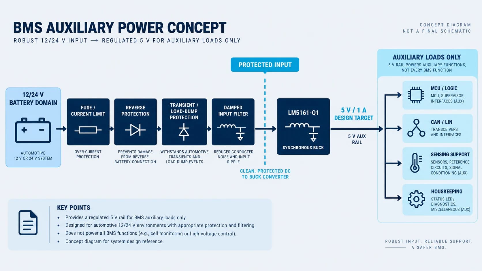
| R06 | BMS Auxiliary Power Reference Design | /reference-designs/bms-auxiliary-power-supply/ | RESOLVED_LINK |
| R07 | Selecting a Buck Converter for Automotive Power | /resources/technical-guides/select-buck-converter-automotive/ | RESOLVED_LINK |
| R08 | Request a Design | /request-a-design/ | RESOLVED_LINK |
| R09 | LM5164-Q1 Component Guide | Plain text only; no published page exists | EXPLICIT_NO_LINK |
| R10 | Automotive always-on and sleep-current budgeting | Editorial discovery only | DISCOVERY_ONLY |
| R11 | Localized RD11 editions | No placeholder ES/PT/FR/RU/AR routes | DEFERRED |
14
Official sources and evidence provenance
Nine first-party Texas Instruments sources support the selected-device facts, orderable identity, evaluation context, design equations and candidate comparison. Vendor information remains attributed; all RD11 numerical design results are separately labeled Hengshun calculations.
15
Related public engineering context
The reviewed links connect RD11 to DC-DC conversion, power protection, Automotive, ECU Power, two complementary reference designs and the published automotive buck-selection guide. Engineers can use Request a Design to provide the protected-node contract, standby-current budget, ambient range and load profile. The missing LM5164-Q1 guide and untranslated editions are intentionally not fabricated.